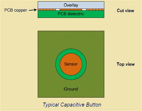
Introduction to PCB Capacitance
Printed Circuit Board (PCB) design is a complex process that involves various electrical and mechanical considerations. One of the critical aspects of PCB design is the management of capacitance between traces and planes. Understanding and accurately calculating the PCB Trace to plane capacitance is essential for ensuring signal integrity, minimizing crosstalk, and optimizing the overall performance of the PCB.
In this article, we will explore the concept of PCB capacitance, its importance in PCB design, and delve into the formula used to calculate the capacitance between a trace and a plane. We will also discuss the factors that influence PCB capacitance and provide practical tips for managing and optimizing capacitance in PCB designs.
What is PCB Capacitance?
PCB capacitance refers to the electrical property that exists between two conductive surfaces separated by an insulating material, such as the dielectric layer in a PCB. In the context of PCB design, capacitance is often considered between traces and planes, as well as between adjacent traces.
Capacitance is measured in farads (F) and is determined by the geometry of the conductive surfaces, the distance between them, and the properties of the insulating material. The presence of capacitance in a PCB can have both beneficial and detrimental effects on the circuit’s performance, depending on the specific application and design requirements.
Importance of PCB Capacitance in PCB Design
Managing PCB capacitance is crucial for several reasons:
-
Signal Integrity: Excessive capacitance between traces and planes can lead to signal distortion, ringing, and other signal integrity issues. By properly calculating and controlling capacitance, designers can ensure that signals maintain their desired shape and timing.
-
Crosstalk Reduction: Capacitive coupling between adjacent traces can result in crosstalk, where a signal on one trace induces unwanted noise on nearby traces. By minimizing the capacitance between traces, designers can reduce crosstalk and improve the overall signal quality.
-
Impedance Matching: Controlling the capacitance between traces and planes is essential for achieving proper impedance matching. Mismatched impedances can lead to signal reflections, which can cause signal degradation and compromise the performance of high-speed circuits.
-
Power Integrity: Capacitance between power and ground planes can impact the power distribution network’s effectiveness. Adequate capacitance can help stabilize the power supply and reduce noise, while excessive capacitance can lead to increased power consumption and heat generation.
PCB Trace to Plane Capacitance Formula
The capacitance between a PCB trace and a plane can be calculated using the following formula:
C = (ε * A) / d
Where:
– C is the capacitance in farads (F)
– ε is the permittivity of the dielectric material (F/m)
– A is the area of the trace overlapping the plane (m^2)
– d is the distance between the trace and the plane (m)
Permittivity (ε)
Permittivity is a measure of a material’s ability to store electrical energy in an electric field. It is a key factor in determining the capacitance between a trace and a plane. The permittivity of a dielectric material is often expressed as the product of the vacuum permittivity (ε₀) and the relative permittivity (εᵣ) of the material.
ε = ε₀ * εᵣ
The vacuum permittivity (ε₀) is a constant value approximately equal to 8.85 × 10⁻¹² F/m. The relative permittivity (εᵣ) is a dimensionless number that represents the ratio of the material’s permittivity to the vacuum permittivity. The relative permittivity of common PCB dielectric materials is shown in the table below:
| Material | Relative Permittivity (εᵣ) |
|---|---|
| Air | 1.0 |
| FR-4 | 4.2 – 4.5 |
| Rogers RO4003C | 3.38 |
| Polyimide | 3.5 |
| Teflon | 2.1 |
Area (A)
The area (A) in the capacitance formula refers to the overlapping area between the trace and the plane. It is determined by the length and width of the trace segment that is directly above or below the plane. The area can be calculated using the following formula:
A = L * W
Where:
– L is the length of the trace segment overlapping the plane (m)
– W is the width of the trace (m)
Distance (d)
The distance (d) in the capacitance formula represents the separation between the trace and the plane. In a typical PCB Stackup, this distance is determined by the thickness of the dielectric layer between the trace and the plane. The distance can be obtained from the PCB Manufacturer’s specifications or by measuring the thickness of the dielectric layer.

Factors Influencing PCB Capacitance
Several factors can influence the capacitance between a trace and a plane in a PCB design. Understanding these factors is essential for effectively managing and optimizing capacitance.
Dielectric Material Properties
The choice of dielectric material significantly impacts the capacitance between a trace and a plane. As discussed earlier, the relative permittivity (εᵣ) of the dielectric material directly affects the capacitance value. PCB designers should select dielectric materials with appropriate permittivity values based on the specific requirements of their application.
Trace Geometry
The geometry of the trace, including its width and length, influences the capacitance between the trace and the plane. Wider traces will have a larger overlapping area with the plane, resulting in higher capacitance. Similarly, longer trace segments that run parallel to a plane will have a greater capacitance compared to shorter segments.
Plane Size and Proximity
The size of the reference plane and its proximity to the trace also affect the capacitance. A larger plane area will result in higher capacitance, as there is more overlapping area between the trace and the plane. Additionally, the closer the plane is to the trace, the higher the capacitance will be, as the distance (d) in the capacitance formula is reduced.
Stackup Configuration
The PCB stackup configuration, which defines the arrangement of layers in the PCB, plays a role in determining the capacitance between traces and planes. The number of layers, their order, and the spacing between them can all impact the capacitance values. Designers should carefully consider the stackup configuration to ensure optimal capacitance management.

Managing and Optimizing PCB Capacitance
Effective management and optimization of PCB capacitance are crucial for achieving reliable and high-performance PCB designs. Here are some strategies and techniques for managing capacitance:
Proper Trace Routing
Careful trace routing is essential for minimizing unwanted capacitance. Designers should avoid running traces parallel to planes for extended distances, as this can increase the overlapping area and lead to higher capacitance. Instead, traces should be routed perpendicular to planes whenever possible to minimize the capacitive coupling.
Adjusting Trace Width and Spacing
Modifying the width and spacing of traces can help control capacitance. Narrower traces will have less overlapping area with the plane, resulting in lower capacitance. Additionally, increasing the spacing between adjacent traces can reduce the capacitive coupling between them, mitigating crosstalk issues.
Selecting Appropriate Dielectric Materials
Choosing the right dielectric material is crucial for managing capacitance. Designers should select materials with suitable permittivity values based on the desired capacitance levels and the specific requirements of the application. Low-permittivity materials, such as Teflon or certain Rogers materials, can be used to reduce capacitance in critical areas of the PCB.
Optimizing Stackup Design
The PCB stackup design should be optimized to control capacitance effectively. Designers can adjust the spacing between layers, use multiple ground planes to provide shielding, and strategically place power and ground planes to minimize unwanted capacitance. Consultation with the PCB manufacturer and adherence to industry standards can help ensure an optimal stackup configuration.
Simulation and Modeling
Utilizing simulation and modeling tools can provide valuable insights into the capacitance behavior of a PCB design. These tools allow designers to analyze the capacitance between traces and planes, identify potential issues, and make informed decisions to optimize the design. Simulations can help predict signal integrity problems, crosstalk, and other capacitance-related effects before the PCB is manufactured.

Frequently Asked Questions (FAQ)
-
What is the typical range of capacitance values in a PCB?
The typical range of capacitance values in a PCB can vary depending on the specific design and application. However, capacitance values in the range of picofarads (pF) to nanofarads (nF) are common. For example, the capacitance between a trace and a plane can be in the order of a few picofarads per centimeter of trace length. -
How does the Dielectric Constant of the PCB material affect capacitance?
The dielectric constant, also known as relative permittivity (εᵣ), is a measure of a material’s ability to store electrical energy in an electric field. A higher dielectric constant indicates a greater capacity to store electrical energy, resulting in higher capacitance. PCB Materials with higher dielectric constants, such as FR-4, will exhibit higher capacitance compared to materials with lower dielectric constants, like Teflon. -
Can PCB capacitance be used intentionally in circuit design?
Yes, PCB capacitance can be intentionally used in circuit design for various purposes. For example, intentional capacitance can be introduced between power and ground planes to create a distributed capacitance network that helps stabilize the power supply and reduce high-frequency noise. Additionally, controlled capacitance can be used in certain applications, such as filters or impedance matching networks, to achieve desired circuit behavior. -
What are some common issues caused by excessive PCB capacitance?
Excessive PCB capacitance can lead to several issues, including: - Signal integrity problems: Excessive capacitance can cause signal distortion, ringing, and overshoot, compromising the quality and reliability of signals.
- Crosstalk: High capacitance between adjacent traces can result in crosstalk, where signals from one trace couple onto nearby traces, causing interference and noise.
- Impedance mismatch: Uncontrolled capacitance can lead to impedance mismatches, resulting in signal reflections and degraded signal quality.
-
Power integrity issues: Excessive capacitance in the power distribution network can impact the stability and noise performance of the power supply.
-
How can PCB designers minimize the impact of capacitance in high-speed designs?
To minimize the impact of capacitance in high-speed PCB designs, designers can employ several techniques: - Use controlled impedance traces: Designing traces with well-defined and matched impedances can help mitigate the effects of capacitance and ensure proper signal propagation.
- Implement proper grounding and shielding: Effective grounding strategies and the use of shielding techniques, such as ground planes and guard traces, can help reduce unwanted capacitance and crosstalk.
- Optimize trace routing: Careful trace routing, such as minimizing parallel runs and using diagonal or curved traces, can help reduce capacitive coupling between traces and planes.
- Select suitable dielectric materials: Choosing PCB materials with lower dielectric constants can help reduce the overall capacitance in the design.
- Perform simulations and analysis: Utilizing simulation tools and conducting thorough analysis of the PCB design can help identify and address capacitance-related issues early in the design process.
Conclusion
Understanding and managing PCB trace to plane capacitance is essential for designing reliable and high-performance PCBs. The capacitance formula, along with knowledge of the factors influencing capacitance, provides designers with the tools to calculate and optimize capacitance values in their designs.
By considering the dielectric material properties, trace geometry, plane size and proximity, and stackup configuration, designers can effectively control capacitance and mitigate issues such as signal integrity problems, crosstalk, and impedance mismatches.
Employing strategies such as proper trace routing, adjusting trace width and spacing, selecting appropriate dielectric materials, optimizing stackup design, and utilizing simulation and modeling tools, designers can manage and optimize PCB capacitance for their specific applications.
As PCB technology continues to advance and signal speeds increase, the importance of understanding and controlling PCB capacitance becomes even more critical. By mastering the concepts and techniques presented in this article, PCB designers can create robust and reliable designs that meet the ever-growing demands of modern electronics.

Leave a Reply