What Are Vias in PCBs?
Vias are small holes drilled through a printed circuit board (PCB) that allow signals and power to pass from one layer of the board to another. They are essential interconnects that enable PCB designers to route traces on different layers to avoid crossing traces, make efficient use of board space, and meet density requirements.
There are several types of vias used in PCBs:
| Via Type | Description |
|---|---|
| Through Hole Via | Drilled through the entire board, can be used to mount through-hole components |
| Blind Via | Connects an outer layer to an inner layer, but does not go through the entire board |
| Buried Via | Connects two or more inner layers, does not extend to outer layers |
| Microvia | A small via, typically laser drilled, used for high density interconnects |
While vias enable routing between layers, they also create some challenges. Exposed vias can lead to soldering and assembly issues, impact signal integrity, and provide openings for contaminants to enter the board. This is where Via covering comes into play.
What is Via Covering?
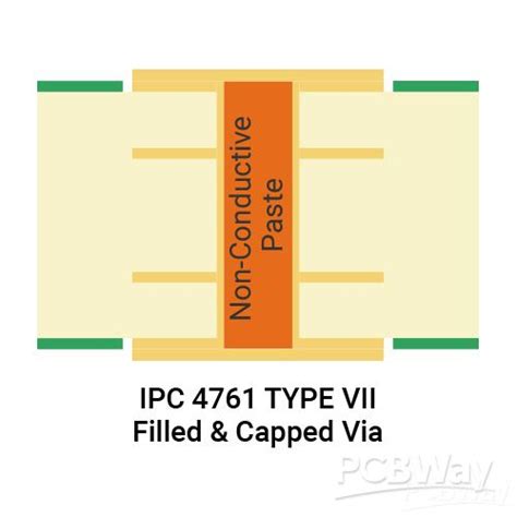
Via covering, also known as via capping, Via Filling, or via plugging, is a PCB manufacturing process that seals the top and/or bottom openings of vias with a non-conductive material. The primary purpose is to cover any exposed via holes, creating a smooth, flat surface on the outer layers of the board.
The via covering process typically involves applying a mask or resin material over the vias, then scraping or sanding the surface to remove any excess and planarize the board. The end result is a PCB with no visible via openings on the top and/or bottom layers.
Via Covering vs Via Filling
While the terms are sometimes used interchangeably, via covering and via filling are slightly different processes:
- Via covering seals the openings on the top and/or bottom layers, but leaves an air gap inside the via barrel
- Via filling uses a conductive or non-conductive material to completely fill the via barrel from top to bottom
In general, via covering is used more for surface mount assembly and aesthetic reasons, while via filling is used for thermal management, high-speed signaling, or impedance control. However, both serve to eliminate exposed via openings.

Benefits of Via Covering
Covering vias on a PCB provides several important benefits for manufacturing, assembly, and reliability:
Improved Solderability
Exposed vias can cause issues during solder paste printing and reflow soldering of surface mount components. If there are open vias near SMT pads, solder paste can flow down into the vias, robbing solder from the component leads. This can lead to poor solder joints or even completely missing solder connections.
By covering the vias, the solder mask provides a barrier to prevent Solder Wicking and ensures proper solder volume on the SMT pads. This improves manufacturing yield and reduces soldering defects.
Better Surface Planarity
Covering vias creates a flatter, more planar surface on the Outer PCB layers. This is critical for fine-pitch surface mount assembly, as even small surface irregularities can cause component misalignment or poor solder joints.
A planar surface also enables the use of smaller stencil apertures for solder paste printing, allowing tighter geometries. Planar substrates are also essential for flip-chip and ball grid array (BGA) assembly to ensure proper solder ball collapse and joint formation.
Reduced Contamination
Exposed vias, especially those that extend all the way through the board, provide openings for flux, cleaning chemistries, and other contaminants to enter the PCB during assembly. Contaminants can migrate through the board and cause corrosion or dendrite growth over time, degrading reliability.
Covering the vias helps seal the board and prevent liquid and gaseous contaminants from penetrating into the PCB. This is especially important in harsh environment applications where the assembly may be exposed to moisture, chemicals, or extreme temperatures.
Improved High-Frequency Performance
At high frequencies, vias can act as resonant cavities or stubs that cause signal reflections and distortions. The impedance discontinuity presented by an open via barrel can degrade signal integrity on high-speed nets like DDRx and SerDes interfaces.
While via filling is the typical solution for high-speed applications, via covering can also help mitigate the stub effect by shortening the resonant cavity. Covering vias is often used in combination with back-drilling to remove the unused portion of the via barrel.
Enhanced Aesthetics
Finally, via covering provides a cleaner, more professional appearance on the outer layers of the PCB. This is important for consumer electronics and other products where cosmetic blemishes are unacceptable.
Covered vias give the board a uniform look without any exposed via holes. Via covering can also enable the addition of silkscreen logos, part markings, or other graphics on the outer layers without the interference of exposed vias.

Via Covering Process
The via covering process is typically performed towards the end of the PCB fabrication process, after the vias are drilled and plated but before the final solder mask and surface finish are applied.
Mask Application
The first step is to apply a mask material over the via openings. This is typically a liquid photoimageable (LPI) solder mask or a dry film solder mask.
For LPI, the liquid mask is coated onto the surface of the board and then exposed and developed to cure the mask and reveal the areas to be covered. For dry film, a solid film is laminated onto the board surface and then photoimaged to define the coverage area.
Curing
After the mask is applied and patterned, it must be cured to harden the material and ensure good adhesion to the board surface. Curing is typically done with UV light and/or heat, depending on the specific mask material.
Proper curing is critical to prevent the mask from peeling or flaking off during subsequent processing steps or during assembly and use.
Planarization
Once the mask is cured, the board surface must be planarized to remove any excess mask material and ensure a flat, level surface. This is typically done by sanding or grinding the surface until it is smooth and all via openings are completely covered.
The planarization step also helps to control the final thickness of the solder mask over the vias. Insufficient mask thickness can lead to incomplete coverage, while excess thickness can cause issues with solder mask alignment or component assembly.
Cleaning
After planarization, the board is cleaned to remove any dust or debris from the sanding process. This is typically done with a high-pressure water wash or a mild chemical cleaning agent.
Thorough cleaning is important to ensure good adhesion of the final solder mask and to prevent any contamination that could cause issues during assembly or reliability testing.
Final Solder Mask and Finish
Once the via covering process is complete, the board moves on to the final solder mask and surface finish stages. The final solder mask is applied over the entire board, including the covered vias, and then the surface finish (HASL, ENIG, IAg, etc.) is applied to the exposed copper areas.
The via covering process is designed to integrate seamlessly with the standard solder mask and finishing steps, so there is typically no need for any special handling or processing.

Via Covering Materials
There are several different materials that can be used for via covering, each with its own advantages and trade-offs.
LPI Solder Mask
Liquid photoimageable solder mask is one of the most common via covering materials. LPI is a polymer resin that is applied as a liquid, then exposed and developed to cure the material in the desired areas.
LPI provides good adhesion, high dielectric strength, and excellent thermal and chemical resistance. It is also relatively easy to process and can be applied in a variety of thicknesses to meet different coverage requirements.
However, LPI can be more expensive than other mask materials and may require additional processing steps for very thick coverage layers.
Dry Film Solder Mask
Dry film solder mask is another popular via covering option. Dry film is a solid photopolymer that is laminated onto the board surface, then exposed and developed to define the coverage area.
Dry film provides good planarity and can be applied in very thick layers (up to 200 microns or more) for complete via coverage. It also has good adhesion and chemical resistance properties.
However, dry film can be more brittle than LPI and may be more prone to cracking or peeling under stress. It also requires specialized lamination equipment for application.
Epoxy Mask
Epoxy mask is a non-photoimageable material that is screen printed or stenciled onto the board surface to cover the vias. Epoxy is a two-part resin that cures through a chemical reaction, typically with heat.
Epoxy provides excellent adhesion, high dielectric strength, and good thermal and chemical resistance. It can also be applied in very thick layers for complete via coverage.
However, epoxy is not photoimageable, so it requires a separate screen or stencil for patterning. It also has a longer cure time than other mask materials and may require higher processing temperatures.
Conductive Filling
For applications that require electrical connection between layers, conductive via filling materials can be used instead of non-conductive masks. These materials, such as conductive epoxies or sintered metal pastes, are applied into the vias and then cured to create a solid, conductive plug.
Conductive filling provides the benefits of via covering along with the ability to carry electrical signals or currents through the board. However, conductive materials are typically more expensive and require more specialized processing than non-conductive masks.
Via Covering Design Considerations
When designing a PCB with via covering, there are several key factors to consider to ensure the best results:
Via Size and Aspect Ratio
The size of the vias and the aspect ratio (depth to diameter) can affect the ability to completely cover the openings. Smaller vias with higher aspect ratios are generally easier to cover than larger, shallow vias.
For best results, designers should use the smallest via size that is feasible for the design and manufacturing process. High aspect ratio vias (>8:1) may require specialized via filling materials or processes.
Via Placement
The location of vias on the board can also impact the via covering process. Vias that are located close to the edge of the board or near large copper features may be more difficult to cover completely.
Designers should avoid placing vias too close to the board edge or other surface features. A minimum spacing of 0.5-1mm is typically recommended between vias and the board edge or other surface obstructions.
Solder Mask Thickness
The thickness of the solder mask used for via covering can affect the final surface planarity and the ability to completely seal the via openings. Thicker mask layers provide better coverage but may be more difficult to planarize.
Designers should work with their PCB fabricator to determine the optimal solder mask thickness for their design. A minimum thickness of 1-2 mils over the via surface is typically recommended for complete coverage.
Via Fill Material Selection
For designs that require via filling instead of or in addition to via covering, the choice of fill material can impact the performance and reliability of the board.
Conductive fill materials like copper or silver epoxy provide the best electrical performance but are more expensive and may require specialized processing. Non-conductive fill materials like epoxy or resin are cheaper and easier to process but do not provide electrical conductivity.
Designers should select the fill material that best meets the performance, reliability, and cost requirements of their specific application.
Frequently Asked Questions
What is the difference between via covering and via filling?
Via covering seals the top and/or bottom openings of the via with a non-conductive material, while via filling completely fills the via barrel with a conductive or non-conductive material. Via covering is primarily used for surface mount assembly and protection, while via filling is used for thermal management, high-speed signaling, or impedance control.
Can via covering be used on both sides of the board?
Yes, via covering can be applied to both the top and bottom sides of the PCB, depending on the design requirements. This is often done for Through-Hole Vias that extend through the entire board stackup.
How does via covering affect the cost of PCB fabrication?
Via covering does add some additional cost to the PCB fabrication process, as it requires additional materials and processing steps. However, the cost impact is relatively minor compared to the overall board cost, typically less than 10% for most designs.
Can via covering be used with any surface finish?
Yes, via covering is compatible with all common PCB Surface Finishes, including HASL, ENIG, OSP, and immersion silver/tin. The via covering process is typically performed before the final surface finish is applied.
How does via covering compare to other via protection methods?
Via covering provides a simple, cost-effective way to seal via openings and improve surface planarity. Other methods like via tenting or plugging can also be used, but may not provide as complete or consistent coverage. Via filling provides the most complete protection but is typically more expensive and complex than via covering.
Conclusion
Via covering is an important PCB manufacturing process that provides numerous benefits for assembly, reliability, and performance. By sealing via openings with a non-conductive mask material, via covering creates a planar surface for component mounting, prevents solder wicking and contamination, and improves high-frequency signal integrity.
While via covering does add some cost and complexity to the fabrication process, the benefits far outweigh the drawbacks for most applications. As PCB designs continue to push the limits of density and performance, via covering will remain an essential tool for ensuring manufacturability and reliability.
By understanding the via covering process, materials, and design considerations, PCB designers and engineers can make informed decisions about when and how to implement via covering in their designs. With the right approach, via covering can help unlock new levels of PCB performance and functionality.


Leave a Reply