Introduction to PCB Multi-layer Fabrication
Printed Circuit Boards (PCBs) are essential components in modern electronic devices, providing a platform for interconnecting electronic components. As technology advances and devices become more complex, the demand for Multi-layer PCBs has increased significantly. Multi-layer PCBs offer several advantages over single-layer boards, including higher component density, improved signal integrity, and reduced electromagnetic interference (EMI).
The fabrication of multi-layer PCBs involves several critical steps, with Lay-up and Bond being one of the most important processes. Lay-up and bond is the process of stacking and bonding multiple layers of PCB material together to create a cohesive, multi-layer board. This article will delve into the details of the lay-up and bond process, its importance in PCB Fabrication, and the various techniques and materials used.
The Importance of Lay-up and Bond in PCB Fabrication
Lay-up and bond is a crucial step in the fabrication of multi-layer PCBs. It ensures that the multiple layers of the PCB are properly aligned, bonded, and able to function as a single, cohesive unit. The process directly affects the following aspects of PCB performance:
-
Signal integrity: Proper lay-up and bond ensures that the signal paths between layers are correctly aligned, minimizing signal distortion and loss.
-
Mechanical stability: A well-executed lay-up and bond process results in a PCB with high mechanical strength and durability, able to withstand the rigors of assembly and use.
-
Thermal management: Efficient heat dissipation is critical in high-density, multi-layer PCBs. Lay-up and bond plays a role in ensuring proper thermal conductivity between layers.
-
Reliability: A PCB with a strong and stable bond between layers is less likely to experience delamination or other failures, resulting in a more reliable end product.

The Lay-up and Bond Process
The lay-up and bond process consists of several steps, each of which must be carefully controlled to ensure the quality of the final product. The main steps include:
1. Material Preparation
The first step in the lay-up and bond process is to prepare the PCB materials. This includes:
- Cleaning: The inner layer and prepreg materials are cleaned to remove any contaminants that may affect the bonding process.
- Tooling: The layers are punched or drilled with tooling holes, which are used to align the layers during the lay-up process.
- Oxide treatment: The inner layers undergo an oxide treatment to improve adhesion during bonding.
2. Lay-up
The lay-up process involves stacking the prepared PCB Layers in the correct order and orientation. The stack typically consists of alternating layers of core material (pre-etched and plated inner layers) and prepreg (pre-impregnated fiberglass sheets).
The lay-up order is determined by the PCB design and Layer Stack-Up specification. Copper foils are placed on the top and bottom of the stack to form the outer layers of the PCB.
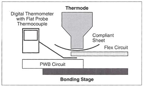
3. Vacuum Press and Bonding
Once the layers are stacked, they are placed in a vacuum press for bonding. The vacuum press applies heat and pressure to the stack, causing the prepreg to melt and flow, bonding the layers together.
The bonding process typically involves the following steps:
- Vacuum: The stack is placed in a vacuum bag and air is removed to eliminate any trapped air between layers.
- Pressure: The vacuum-sealed stack is placed in a press, where high pressure is applied to ensure intimate contact between layers.
- Heat: The press is heated to the bonding temperature, typically between 180°C and 200°C, depending on the prepreg material used.
- Cooling: After the bonding cycle, the stack is cooled under pressure to ensure a strong, stable bond.
The specific parameters for the bonding process, such as temperature, pressure, and time, depend on the materials used and the thickness of the PCB.
4. Inspection and Testing
After the lay-up and bond process, the PCB undergoes inspection and testing to ensure the quality of the bond and the integrity of the circuit. Common tests include:
- Visual inspection: The PCB is visually inspected for any signs of delamination, blistering, or other defects.
- Microsectioning: A cross-section of the PCB is examined under a microscope to verify the integrity of the bond between layers.
- Electrical testing: The PCB is subjected to electrical tests to ensure that the circuits are functioning correctly and that there are no shorts or opens between layers.

Materials Used in Lay-up and Bond
The choice of materials used in the lay-up and bond process is critical to the success of the final product. The main materials used include:
1. Core Materials
Core materials are the pre-etched and plated inner layers of the PCB. They are typically made of FR-4, a type of fiberglass-reinforced epoxy laminate. Other materials, such as polyimide or high-frequency laminates, may be used for specialized applications.
2. Prepreg
Prepreg (pre-impregnated) is a sheet of fiberglass impregnated with a partially cured epoxy resin. It is used as the bonding agent between the core layers. The properties of the prepreg, such as resin content and flow characteristics, are selected based on the specific requirements of the PCB, such as layer count, thickness, and required bond strength.
3. Copper Foil
Copper foil is used to form the outer layers of the PCB. The foil thickness is selected based on the desired current-carrying capacity and the requirements of the circuit design. Copper foil is available in various grades and surface treatments to optimize adhesion and signal integrity.

Advanced Techniques in Lay-up and Bond
As PCB technology continues to evolve, new techniques and materials are being developed to improve the lay-up and bond process. Some of these advanced techniques include:
1. Thermally Conductive Prepregs
For applications that require enhanced thermal management, thermally conductive prepregs can be used. These prepregs contain thermally conductive fillers, such as ceramic particles or carbon nanotubes, that improve the thermal conductivity of the PCB, helping to dissipate heat more effectively.
2. Low-loss Materials
In high-frequency applications, signal loss and distortion can be a significant problem. Low-loss materials, such as hydrocarbon ceramic laminates or polytetrafluoroethylene (PTFE) based laminates, can be used to reduce signal loss and improve signal integrity.
3. Embedded Components
Embedded components, such as capacitors or resistors, can be integrated into the PCB Stack-up during the lay-up process. This technique can save space, reduce the number of external components, and improve signal integrity by reducing the length of signal paths.
Conclusion
Lay-up and bond is a critical process in the fabrication of multi-layer PCBs. It directly affects the performance, reliability, and durability of the final product. By understanding the importance of lay-up and bond, the steps involved in the process, and the materials used, PCB designers and manufacturers can ensure the production of high-quality, reliable multi-layer PCBs.
As PCB technology continues to advance, new techniques and materials are being developed to improve the lay-up and bond process, enabling the production of increasingly complex and high-performance multi-layer PCBs.
Frequently Asked Questions (FAQ)
-
What is the purpose of the oxide treatment in the material preparation stage?
The oxide treatment improves the adhesion between the core layers and the prepreg during the bonding process. The treatment creates a rough surface on the copper, increasing the surface area for the prepreg to bond to. -
What is the role of the vacuum in the bonding process?
The vacuum is used to remove any trapped air between the layers of the PCB stack. Trapped air can cause voids or delamination in the final product, compromising its integrity and reliability. -
What is the difference between core materials and prepreg?
Core materials are the pre-etched and plated inner layers of the PCB, while prepreg is the bonding agent used between the core layers. Core materials provide the structure and the conductive paths for the circuit, while prepreg ensures a strong, stable bond between the layers. -
How does the choice of prepreg affect the performance of the PCB?
The properties of the prepreg, such as resin content and flow characteristics, can affect the bond strength, thermal conductivity, and signal integrity of the PCB. The choice of prepreg depends on the specific requirements of the PCB, such as layer count, thickness, and operating conditions. -
What are the benefits of using embedded components in the lay-up and bond process?
Embedded components can save space, reduce the number of external components, and improve signal integrity by reducing the length of signal paths. By integrating components into the PCB stack-up, designers can create more compact and efficient PCBs for high-performance applications.
| Material | Function | Properties |
|---|---|---|
| Core (FR-4) | Inner layers of PCB | Fiberglass-reinforced epoxy laminate |
| Prepreg | Bonding agent between core layers | Fiberglass sheet impregnated with partially cured epoxy resin |
| Copper Foil | Outer layers of PCB | Available in various thicknesses and surface treatments |


Leave a Reply