Introduction to PCB Milling
PCB milling is a subtractive manufacturing process used in printed circuit board (PCB) fabrication where a rotating cutting tool removes copper from a copper-clad substrate to create the traces, pads, and vias that electrically connect components on the board. It is an alternative to traditional chemical etching processes for PCB Prototyping and low-volume production.
In the PCB milling process, a computer numerical control (CNC) machine precisely moves the cutting tool in the X, Y, and Z axes based on instructions from computer-aided manufacturing (CAM) software. This allows for quick iterations and design changes without the need for masks or chemicals.
Advantages of PCB Milling
- Rapid prototyping
- No chemicals or masks required
- Easy design changes
- Suitable for low-volume production
- Allows for unique board shapes and cutouts
Disadvantages of PCB Milling
- Slower than chemical etching for high volumes
- Limited trace width and spacing compared to etching
- Higher cost per board for large quantities
- Not well-suited for plated through holes
The PCB Milling Process
Step 1: PCB Design
The PCB milling process begins with designing the circuit board using electronic design automation (EDA) or PCB design software. The design specifies the size and shape of the board, component placement, trace routing, drill holes, and more.
Step 2: CAM File Generation
Once the PCB design is complete, it is exported to a CAM file format such as Gerber or Excellon. These files contain instructions for the CNC milling machine on where to route traces, drill holes, and cut the board outline.
Step 3: Substrate Preparation
A copper-clad substrate, typically FR-4 glass-reinforced epoxy laminate, is cut to the appropriate size for the PCB design. The substrate is then cleaned to remove any surface contaminants that could interfere with copper adhesion or cause uneven milling.
Step 4: Substrate Mounting
The prepared substrate is securely mounted to the CNC milling machine’s work surface using tape, vacuum, or mechanical clamps to prevent shifting during the milling process. Proper mounting is critical for achieving accurate feature sizes and positions.
Step 5: Tool Selection and Loading
The CNC machine operator selects the appropriate cutting tools for the job based on the minimum trace width, via diameter, and other design requirements specified in the CAM files. Common tool types and sizes for PCB milling include:
| Tool Type | Diameter Range (mm) | Typical Use |
|---|---|---|
| End Mill | 0.1 – 3.0 | Traces, pads, cutouts |
| Drill Bit | 0.2 – 6.3 | Vias, through holes |
| V-Groove | 0.1 – 0.4 (tip) | Breakaway tabs, scoring |
The selected tools are loaded into the CNC machine’s spindle and tool changer, and their lengths and diameters are measured to ensure proper offset compensation during milling.
Step 6: Milling Operation
With the substrate mounted and tools loaded, the CNC machine executes the CAM file instructions to mill away unwanted copper, leaving behind the desired traces, pads, and features. The milling operation typically proceeds in the following order:
- Drill holes and vias
- Isolation routing (clearing copper between traces)
- Rubout (removing bulk copper)
- Board outline cutting
Depending on the design complexity and tool sizes, the milling operation can take anywhere from a few minutes to several hours to complete.
Step 7: Cleaning and Inspection
After milling, the PCB is removed from the machine and cleaned with compressed air, alcohol, or a mild detergent solution to remove copper chips and dust. The board is then visually inspected under magnification to check for defects such as:
- Incomplete traces or pads
- Shorts between traces
- Burrs or rough edges
- Incorrect hole sizes or positions
If any defects are found, the board may need to be reworked or scrapped, and the milling process repeated with adjustments to the design, tools, or machine settings.
Step 8: Surface Finish Application (Optional)
For improved solderability, oxidation resistance, and aesthetics, the milled PCB can be plated or coated with a surface finish such as:
- Hot air solder leveling (HASL)
- Immersion Silver, tin, or gold
- Organic solderability preservatives (OSP)
Surface finish application involves additional processing steps such as cleaning, activation, plating, and curing, which may be outsourced to a specialized PCB finishing provider.

PCB Milling Machine Types and Features
PCB milling machines come in a range of sizes, capabilities, and price points to suit different prototyping and production needs. Some common types and features include:
Benchtop PCB Milling Machines
Compact, entry-level machines for hobbyists, educators, and small labs. Typically have a working area of 100-500 cm² and spindle speeds up to 50,000 RPM. Examples:
- LPKF ProtoMat S series
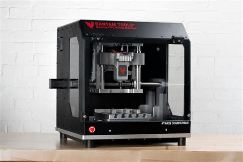
- Bantam Tools Desktop PCB Milling Machine
- WEGSTR iM0609 CNC Router Machine
High-Speed PCB Milling Machines
Professional-grade machines with higher spindle speeds (up to 150,000 RPM), faster feed rates, and more rigid construction for improved accuracy and throughput. Often have automatic tool changers and vacuum tables. Examples:
- LPKF ProtoMat E series
- Accurate CNC A406 High Speed PCB Router
- JCUT-6090 CNC Router
Multi-Spindle PCB Milling Machines
Production-oriented machines with multiple spindles that can mill several PCBs simultaneously for increased output. May have features like automatic substrate handling and unloading. Examples:
- LPKF ProtoMat D104
- MPS1200 4-Axis CNC PCB Router
Key PCB Milling Machine Features
- Spindle speed and power
- Axis travel and resolution
- Tool change system (manual, semi-automatic, or fully automatic)
- Substrate clamping method (tape, vacuum, mechanical)
- Dust collection and cooling systems
- CAM software compatibility and ease of use

Optimizing PCB Milling Results
To achieve the best possible results from your PCB milling process, consider the following tips and guidelines:
Design for Manufacturability (DFM)
- Use appropriate trace widths and spacings for your milling tools and substrate
- Avoid sharp angles and narrow necks in traces to prevent tool breakage
- Provide adequate clearance around holes and board edges
- Follow your PCB manufacturer’s design rules and guidelines
Substrate Selection
- Choose a substrate with good dimensional stability and machinability, such as FR-4
- Consider using a thicker substrate (1.6 mm or more) for better rigidity and edge quality
- For high-frequency or impedance-controlled designs, use a substrate with a tight dielectric constant tolerance
Tool Selection and Management
- Use the largest possible tool diameter that still meets your trace width and spacing requirements to minimize milling time
- Select tools with high-quality carbide or diamond coatings for longer life and better finish quality
- Regularly inspect and replace worn or damaged tools to avoid defects and maintain consistency
- Keep track of tool usage and order replacements before they are needed
Spindle Speed and Feed Rate Optimization
- Use the manufacturer’s recommended spindle speed range for each tool diameter and material type
- Adjust feed rates based on factors like substrate hardness, tool wear, and desired surface finish
- Perform test cuts on scrap material to find the optimal speeds and feeds for your specific job
- Monitor spindle load and adjust parameters as needed to avoid tool breakage or overheating
Chip Evacuation and Cooling
- Use compressed air or vacuum to remove chips from the cutting area and prevent recutting
- Apply a mist or spray coolant to lubricate the cutting tool and dissipate heat, especially for dense designs or hard substrates
- Clean the PCB thoroughly after milling to remove any embedded chips or debris

Choosing a PCB Milling Service
If you don’t have access to a PCB milling machine or prefer to outsource your prototyping and production needs, there are many PCB milling services available online and locally. When choosing a service, consider factors such as:
Capabilities and Equipment
- Minimum trace width and spacing supported
- Maximum board size and layer count
- Available surface finishes and substrates
- Turnaround time and rush options
Quality and Reliability
- ISO or other quality certifications held
- Customer reviews and testimonials
- Defect rate and warranty policy
- Experience with your specific industry or application
Cost and Value
- Price per board or square inch
- Volume discounts and setup fees
- Shipping costs and options
- Customer support and technical assistance provided
Some popular online PCB milling services include:
- OSH Park
- JLCPCB
- PCBWay
- Seeed Studio Fusion
- ExpressPCB
For local providers, search online directories or ask for recommendations from colleagues, suppliers, or industry associations in your area.
Conclusion
PCB milling is a versatile and efficient method for prototyping and low-volume production of printed circuit boards. By using a CNC machine to selectively remove copper from a substrate, PCB designers can quickly iterate and test their designs without the need for masks or chemicals.
While PCB milling has some limitations compared to traditional etching processes, such as slower speed and higher cost for large volumes, it offers many advantages for rapid prototyping, design flexibility, and ease of use.
By understanding the basics of the PCB milling process, machine types and features, and optimization techniques, you can make informed decisions about whether this method is right for your PCB fabrication needs. And if you choose to outsource your milling work, knowing what to look for in a quality service provider can help you get the best results for your budget and timeline.
FAQ
1. What is the minimum trace width and spacing achievable with PCB milling?
The minimum trace width and spacing depend on the specific PCB milling machine, tools, and substrate used, but typically range from 0.1 to 0.5 mm (4 to 20 mils). High-end machines with fine-tipped tools can achieve even smaller features, while entry-level machines may be limited to 0.2 mm or larger.
2. How much does a PCB milling machine cost?
PCB milling machine prices vary widely based on features, size, and capabilities, from around $500 for a basic benchtop model to over $100,000 for a high-end production machine. Mid-range machines suitable for professional prototyping and low-volume production typically cost between $5,000 and $50,000.
3. Can PCB milling be used for multilayer boards?
Yes, PCB milling can be used to fabricate multilayer boards by milling and stacking individual layers with prepreg or adhesive between them, then laminating the stack together under heat and pressure. However, the alignment and registration of layers can be more challenging with milling compared to traditional etching processes.
4. How long does it take to mill a typical PCB?
The milling time for a PCB depends on factors such as the board size, complexity, number of layers, and machine specifications. A simple single-sided board can be milled in a few minutes, while a complex multilayer board with fine features may take several hours. Typical milling times for a medium-complexity double-sided board range from 15 minutes to 2 hours.
5. What software is used for PCB milling?
PCB milling machines typically use CAM (computer-aided manufacturing) software to convert PCB designs into toolpaths and instructions for the CNC machine. Some popular PCB milling CAM software packages include:
- FlatCAM
- EAGLE CAM Processor
- CircuitCAM
- KiCAM
- MeshCAM
Many PCB design and EDA software tools also have built-in or add-on CAM processors for generating milling files from PCB layouts.


Leave a Reply