Introduction to PCB Files
A PCB file, short for Printed Circuit Board file, is a digital document that contains all the necessary information required to design and manufacture a printed circuit board. These files are essential in the electronics industry as they enable the creation of complex electronic circuits on a single board, making devices more compact, efficient, and reliable.
What is a Printed Circuit Board?
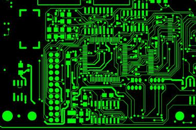
A printed circuit board (PCB) is a flat board made of insulating materials, such as fiberglass or plastic, with conductive copper traces etched onto its surface. These traces connect various electronic components, such as resistors, capacitors, and integrated circuits (ICs), to form a complete electronic circuit. PCBs are used in almost all electronic devices, from simple gadgets like calculators and digital clocks to complex systems like computers and smartphones.
The Importance of PCB Files
PCB files play a crucial role in the design and manufacturing process of printed circuit boards. They contain all the necessary information, including the board layout, component placement, and routing of the conductive traces. Without these files, it would be impossible to create a functional PCB that meets the specific requirements of an electronic device.
Types of PCB Files
There are several types of PCB files, each serving a specific purpose in the design and manufacturing process. Some of the most common types include:
1. Gerber Files
Gerber files, also known as RS-274X files, are the most widely used format for PCB design. They contain information about the copper layers, solder mask, silkscreen, and drill holes of a PCB. Gerber files are text-based and use a specific set of commands to describe the layout of the board.
Example of a Gerber File
G04 Gerber RS-274X file*
%FSLAX24Y24*%
%MOMM*%
%ADD10C,0.1000*%
D10*
X1000Y1000D02*
X2000Y2000D01*
M02*
In this example, the Gerber file defines a simple line segment starting at coordinates (10.00mm, 10.00mm) and ending at (20.00mm, 20.00mm) using aperture D10, which is a circular aperture with a diameter of 1.00mm.
2. Drill Files
Drill files, also known as NC drill files or Excellon files, contain information about the location and size of the drill holes on a PCB. These files are used by CNC (Computer Numerical Control) machines to drill the holes accurately.
Example of a Drill File
M48
METRIC,000.000
T01C0.80
T02C1.00
%
T01
X010000Y010000
X020000Y020000
T02
X030000Y030000
X040000Y040000
M30
In this example, the drill file defines two types of drill holes: T01 with a diameter of 0.80mm and T02 with a diameter of 1.00mm. The file then specifies the coordinates of the drill holes for each type.
3. ODB++ Files
ODB++ (Open Database++) is a comprehensive PCB file format that includes all the necessary information for PCB manufacturing, such as copper layers, drill data, and component placement. ODB++ files are more compact and efficient than Gerber files, as they store all the data in a single, unified database.
4. IPC-2581 Files
IPC-2581 is an open, neutral format for exchanging PCB design data. It is designed to be more intelligent and efficient than Gerber files, as it includes additional information such as net connectivity, component attributes, and design intent.

PCB design software and File Formats
There are numerous PCB design software packages available, each with its own native file format. However, most of these software tools can import and export PCB files in various standard formats, such as Gerber, ODB++, and IPC-2581. Some of the popular PCB design software include:
| Software | Company | Native File Format |
|---|---|---|
| Altium Designer | Altium | .PcbDoc |
| Eagle | Autodesk | .brd |
| KiCad | KiCad | .kicad_pcb |
| OrCAD | Cadence | .brd |
| PADS | Mentor Graphics | .pcb |
It is essential to choose a PCB design software that supports the file formats required by your PCB manufacturer and can export files in a format that is compatible with their manufacturing process.

The PCB Design and Manufacturing Process
The process of creating a PCB involves several stages, each requiring specific PCB files:
1. Schematic Design
The first step in PCB design is creating a schematic diagram that represents the electrical connections between components. This is typically done using an Electronic Design Automation (EDA) tool, such as Altium Designer or KiCad.
2. PCB layout
Once the schematic is complete, the next step is to create the physical layout of the PCB. This involves placing components on the board and routing the copper traces to connect them according to the schematic. The PCB layout is usually created using the same EDA tool used for the schematic design.
3. Design Rule Check (DRC)
After the PCB layout is complete, it is essential to perform a Design Rule Check (DRC) to ensure that the board meets the manufacturing constraints and design guidelines. The DRC checks for issues such as minimum trace width, clearance between traces, and drill hole sizes.
4. File Generation
Once the PCB layout passes the DRC, the next step is to generate the necessary files for manufacturing. This typically involves exporting Gerber files for each layer of the PCB, as well as drill files for the hole locations and sizes.
5. PCB fabrication
The generated PCB files are then sent to a PCB manufacturer, who uses them to fabricate the physical board. The manufacturer will use the Gerber files to create the copper layers and the drill files to drill the necessary holes.
6. PCB Assembly
After the PCB is fabricated, the electronic components are soldered onto the board according to the component placement information in the PCB files. This process can be done manually or using automated assembly machines.

Best Practices for Creating PCB Files
To ensure that your PCB files are accurate and compatible with your manufacturer’s requirements, follow these best practices:
- Use a consistent naming convention for your files, including the board name, version number, and file type.
- Include all necessary layers in your Gerber files, such as copper layers, solder mask, and silkscreen.
- Ensure that your drill files are in the correct format and include all the necessary hole sizes and locations.
- Verify that your PCB files meet your manufacturer’s design guidelines, such as minimum trace width and clearance.
- Always run a Design Rule Check (DRC) before exporting your PCB files to catch any potential issues.
Frequently Asked Questions (FAQ)
1. What is the difference between Gerber and ODB++ files?
Gerber files are the most widely used format for PCB design and contain information about individual layers of the PCB, such as copper traces, solder mask, and silkscreen. ODB++, on the other hand, is a more comprehensive format that includes all the necessary information for PCB manufacturing in a single, unified database.
2. Can I use different PCB design software to edit an existing PCB file?
It depends on the file format and the compatibility of the software. Most PCB design software can import and export files in standard formats like Gerber and ODB++, allowing you to edit the files using different software. However, it is essential to ensure that the software you are using supports the specific file format and version of the PCB file you want to edit.
3. What should I do if my PCB manufacturer does not support the file format I have?
In most cases, PCB manufacturers will support standard file formats like Gerber and ODB++. If your manufacturer does not support the format you have, you can try exporting your PCB files in a compatible format using your PCB design software. If that is not possible, you may need to consider using a different manufacturer or redesigning your PCB using software that supports the required file format.
4. How can I ensure that my PCB files are error-free?
To minimize the risk of errors in your PCB files, follow best practices such as using a consistent naming convention, including all necessary layers, and running a Design Rule Check (DRC) before exporting your files. Additionally, carefully review your files before sending them to your manufacturer and consider using a PCB file viewer to visually inspect the files for any issues.
5. What happens if there is an error in my PCB files during manufacturing?
If there is an error in your PCB files during manufacturing, it can lead to delays, additional costs, and potential quality issues with your final product. In some cases, the manufacturer may be able to correct minor errors, but more significant issues may require you to revise and resubmit your files. To avoid these problems, ensure that your PCB files are accurate, complete, and compatible with your manufacturer’s requirements before submitting them for production.
Conclusion
PCB files are essential for the design and manufacturing of printed circuit boards, which form the backbone of modern electronic devices. By understanding the different types of PCB files, the design and manufacturing process, and best practices for creating these files, you can ensure that your PCBs are produced accurately and efficiently. When working with PCB files, always consider your manufacturer’s requirements, use compatible software, and thoroughly review your files before submitting them for production. By following these guidelines, you can minimize the risk of errors and delays, ultimately leading to a successful PCB manufacturing experience.


Leave a Reply