What is a Circuit Board?
A circuit board, also known as a printed circuit board (PCB), is a fundamental component in electronic devices. It serves as a base for connecting electronic components using conductive tracks, pads, and other features. Circuit boards are used in a wide range of applications, from simple projects to complex electronic systems.
Benefits of Building Your Own Circuit Boards
Creating your own circuit boards offers several advantages:
- Customization: You have complete control over the design and layout of your circuit board, allowing you to tailor it to your specific needs.
- Cost-effectiveness: Building your own circuit boards can be more cost-effective than purchasing pre-made boards, especially for small-scale projects.
- Learning experience: The process of designing and building circuit boards provides valuable hands-on experience in electronics and PCB Fabrication.

Tools and Materials Required
Before we dive into the steps of building a circuit board, let’s take a look at the tools and materials you’ll need:
| Tools | Materials |
|---|---|
| Soldering iron | Copper-clad board |
| Solder | Etchant solution |
| Multimeter | Drill bits |
| Wire cutters | Electrical components |
| Tweezers | Acetone or rubbing alcohol |
| Safety glasses | Permanent marker |
| Protective gloves | Transfer paper |
1. Designing the Circuit
The first step in building a circuit board is designing the circuit. This involves creating a schematic diagram that represents the electrical connections between components. You can use software tools like KiCad, Eagle, or Altium Designer to create your schematic.
Key Considerations:
- Determine the purpose and functionality of your circuit.
- Select the appropriate components based on your requirements.
- Ensure proper connections between components.
- Consider power supply and grounding.
2. Creating the PCB Layout
Once you have your schematic ready, the next step is to create the PCB layout. This involves translating the schematic into a physical representation of the circuit board. PCB design software helps you arrange components, route traces, and define the board dimensions.
Tips for PCB Layout:
- Keep track widths and spacing consistent.
- Minimize the length of traces to reduce signal interference.
- Provide adequate clearance between components.
- Consider component placement for ease of soldering and assembly.
3. Transferring the Design to the Copper-Clad Board
With your PCB layout complete, it’s time to transfer the design onto the copper-clad board. There are a few methods you can use:
Toner Transfer Method:
- Print the PCB layout on a glossy paper using a laser printer.
- Clean the copper-clad board with acetone or rubbing alcohol.
- Place the printed layout face-down on the copper-clad board.
- Apply heat using an iron to transfer the toner onto the copper.
- Soak the board in water and gently peel off the paper.
UV Exposure Method:
- Print the PCB layout on a transparency film.
- Apply a UV-sensitive resist coating to the copper-clad board.
- Place the transparency film on top of the coated board.
- Expose the board to UV light for the recommended duration.
- Develop the board using the appropriate developer solution.
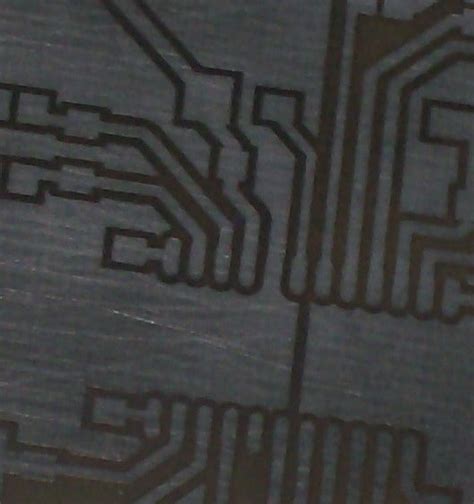
4. Etching the Circuit Board
After transferring the design, the next step is to etch away the unwanted copper, leaving only the desired traces and pads. This is typically done using an etchant solution, such as ferric chloride or ammonium persulfate.
Etching Process:
- Prepare the etchant solution according to the manufacturer’s instructions.
- Immerse the circuit board in the etchant solution.
- Agitate the solution gently to ensure even etching.
- Monitor the etching progress and remove the board once the unwanted copper is dissolved.
- Rinse the board thoroughly with water.
5. Drilling Holes and Soldering Components
With the etching complete, it’s time to drill holes for component leads and mounting. Use a drill press or a hand drill with the appropriate drill bits to create the necessary holes.
After drilling, you can proceed with soldering the components onto the circuit board. Follow these steps:
- Clean the board with isopropyl alcohol to remove any residue.
- Place the components according to the PCB layout.
- Solder the components securely to the pads using a soldering iron and solder.
- Trim any excess component leads.
6. Testing and Troubleshooting
Once you have soldered all the components, it’s crucial to test your circuit board to ensure it functions as intended. Use a multimeter to check for continuity and verify the connections.
If you encounter any issues, here are some troubleshooting tips:
- Double-check your soldering joints for any cold or bridged connections.
- Verify the component values and orientations.
- Ensure proper power supply and grounding.
- Use a magnifying glass to inspect for any short circuits or broken traces.

Frequently Asked Questions (FAQ)
-
What is the best software for designing circuit boards?
There are several popular software options for designing circuit boards, including KiCad, Eagle, and Altium Designer. KiCad is a free and open-source option suitable for beginners, while Eagle and Altium Designer offer more advanced features for professional use. -
Can I use a regular printer for the toner transfer method?
No, it is recommended to use a laser printer for the toner transfer method. Inkjet printers do not produce the necessary toner density and may not transfer the design properly onto the copper-clad board. -
How do I choose the right etchant solution?
The most common etchant solutions are ferric chloride and ammonium persulfate. Ferric chloride is widely available and effective, but it can be messy and stain surfaces. Ammonium persulfate is a cleaner alternative but may require more time for etching. Consider your preferences and safety precautions when choosing an etchant solution. -
What should I do if my circuit board doesn’t work after soldering?
If your circuit board doesn’t function as expected, start by visually inspecting the board for any obvious issues, such as poor soldering joints, short circuits, or damaged components. Use a multimeter to check for continuity and correct connections. If the problem persists, review your schematic and PCB layout to ensure they are accurate. -
Can I reuse the etchant solution?
Yes, you can reuse the etchant solution multiple times until it becomes exhausted. However, keep in mind that the etching process will slow down as the solution weakens. Store the used etchant solution properly and dispose of it according to local regulations when it is no longer effective.

Conclusion
Building your own circuit boards can be a rewarding and educational experience. By following the steps outlined in this guide, you can create Custom PCBs for your electronic projects. Remember to prioritize safety, take your time, and practice patience throughout the process.
As you gain more experience, you can explore advanced techniques and design more complex circuits. The world of DIY Circuit Boards offers endless possibilities for innovation and creativity.
Happy circuit building!


Leave a Reply