Understanding Soldering PCB Defects
Before diving into the methods of checking for defects, let’s first understand what soldering PCB defects are. Soldering PCB defects refer to any imperfections or anomalies that occur during the soldering process, resulting in suboptimal or faulty connections between components and the PCB.
Common Types of Soldering PCB Defects
There are several common types of soldering PCB defects that can occur:
- Bridging: Unintended connections between adjacent pads or traces due to excess solder.
- Cold joints: Weak or brittle solder joints caused by insufficient heat or improper soldering technique.
- Insufficient solder: Inadequate amount of solder, leading to weak or incomplete connections.
- Excessive solder: Too much solder applied, potentially causing short circuits or impeding component placement.
- Lifted Pads: Pads that have detached from the PCB surface due to excessive heat or mechanical stress.
- Tombstoning: Components standing on one end due to uneven heating or surface tension issues.
10 Helpful Ways to Check Defects on Soldering PCB Board
Now that we understand the types of defects that can occur, let’s explore ten helpful ways to check for these defects on soldering PCB boards.
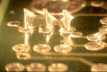
1. Visual Inspection
The first and most basic method of checking for soldering defects is through visual inspection. This involves carefully examining the soldered joints and components using the naked eye or with the aid of magnification tools like a magnifying glass or microscope.
When performing a visual inspection, look for the following:
– Proper alignment of components
– Adequate solder coverage and fillets
– Absence of bridging or short circuits
– Smooth and shiny solder joints
– No visible cracks or gaps in the solder
2. X-Ray Inspection
X-ray inspection is a non-destructive testing method that allows for the examination of solder joints and components beneath the surface of the PCB. This technique is particularly useful for identifying defects in multi-layered boards or in areas where visual inspection is not possible.
X-ray machines generate high-resolution images of the PCB, revealing any voids, cracks, or inconsistencies in the solder joints. This method can detect defects such as:
– Voids in ball grid array (BGA) solder balls
– Insufficient solder in through-hole components
– Misaligned or missing components
– Solder bridges or short circuits
3. Automated Optical Inspection (AOI)
Automated Optical Inspection (AOI) is a computer-based system that uses high-resolution cameras and advanced image processing algorithms to inspect PCBs for defects. AOI systems can quickly scan the entire PCB and compare it against a reference image or design data to identify any anomalies.
AOI systems can detect a wide range of defects, including:
– Incorrect component placement
– Solder bridges or short circuits
– Insufficient or excessive solder
– Missing or damaged components
– Polarity errors
AOI is particularly useful for high-volume production runs, as it can quickly and accurately inspect large numbers of PCBs.
4. In-Circuit Testing (ICT)
In-Circuit Testing (ICT) is a method that involves using specialized test equipment to verify the functionality and connectivity of individual components on the PCB. ICT systems use a bed-of-nails fixture that makes contact with specific test points on the board, allowing for the testing of each component in isolation.
ICT can detect defects such as:
– Open or short circuits
– Incorrect component values
– Missing or damaged components
– Incorrect polarity
– Insufficient or excessive solder
ICT is an effective method for identifying defects that may not be visually apparent and can provide a comprehensive test coverage of the PCB.
5. Flying Probe Testing
Flying probe testing is an alternative to the bed-of-nails approach used in ICT. Instead of using a fixed fixture, flying probe systems utilize movable probes that can be positioned anywhere on the PCB to make contact with test points.
Flying probe testing offers several advantages over traditional ICT:
– Flexibility in testing different PCB designs without the need for custom fixtures
– Ability to test high-density boards with closely spaced components
– Reduced setup time and cost compared to bed-of-nails fixtures
Flying probe systems can detect similar defects as ICT, including open/short circuits, incorrect component values, and soldering issues.
6. Boundary Scan Testing
Boundary scan testing, also known as JTAG (Joint Test Action Group) testing, is a method that utilizes built-in test circuitry within the integrated circuits (ICs) on the PCB. This test circuitry allows for the testing of interconnections between ICs without the need for physical access to the individual pins.
Boundary scan testing can detect defects such as:
– Open or short circuits between ICs
– Stuck-at faults (pins permanently stuck at a logical high or low)
– Incorrect interconnections between ICs
– Defective or non-functional ICs
Boundary scan testing is particularly useful for testing complex, high-density boards with limited physical access to test points.
7. Functional Testing
Functional testing involves testing the PCB as a complete system to verify that it performs its intended function correctly. This type of testing typically requires the PCB to be powered up and connected to any necessary external components or devices.
Functional testing can reveal defects that may not be detected by other methods, such as:
– Incorrect firmware or software
– Timing or synchronization issues
– Intermittent failures due to thermal or mechanical stress
– Compatibility issues with other components or systems
Functional testing is an essential step in ensuring that the PCB meets its design specifications and performs reliably in its intended application.
8. Thermal Imaging
Thermal imaging is a non-contact method that uses infrared cameras to visualize the temperature distribution across the PCB. This technique can help identify areas of excessive heat generation, which may indicate defects such as:
– Overloaded components
– Short circuits
– Insufficient solder coverage
– Poor thermal dissipation
Thermal imaging can also reveal hot spots caused by improper component placement or inadequate cooling, which can lead to premature failure of the PCB.
9. Microsectioning
Microsectioning is a destructive testing method that involves cutting a cross-section of the PCB and examining it under a microscope. This technique allows for the detailed examination of solder joints, component placement, and internal layers of the board.
Microsectioning can reveal defects such as:
– Voids or cracks in solder joints
– Insufficient or excessive solder
– Delamination or separation of PCB Layers
– Plating defects in through-holes or vias
While microsectioning is a destructive method and cannot be used on production boards, it can provide valuable insights into the quality of the soldering process and help identify potential issues.
10. Electrical Testing
Electrical testing involves measuring various electrical parameters of the PCB to ensure that they meet the specified requirements. This can include tests such as:
– Continuity testing: Verifying that there are no open circuits or breaks in the electrical paths.
– Insulation resistance testing: Measuring the resistance between different electrical networks to ensure adequate insulation.
– Dielectric withstanding voltage (DWV) testing: Applying a high voltage to the PCB to check for any leakage or breakdown of the insulation.
– Impedance testing: Measuring the impedance of critical signal paths to ensure they meet the required specifications.
Electrical testing can help identify defects such as:
– Open or short circuits
– Insulation failures
– Impedance mismatches
– Leakage currents
By performing a combination of these electrical tests, you can ensure that the PCB meets its electrical performance requirements and is free from defects that could impact its functionality.

Frequently Asked Questions (FAQ)
-
Q: What are the most common soldering PCB defects?
A: The most common soldering PCB defects include bridging (short circuits), cold joints, insufficient or excessive solder, lifted pads, and tombstoning. -
Q: Can all soldering defects be detected visually?
A: While visual inspection can identify many types of soldering defects, some defects, such as internal voids or cracks, may not be visible to the naked eye. Other testing methods, such as X-ray inspection or microsectioning, may be necessary to detect these hidden defects. -
Q: What is the difference between ICT and flying probe testing?
A: In-Circuit Testing (ICT) uses a fixed bed-of-nails fixture to make contact with specific test points on the PCB, while flying probe testing utilizes movable probes that can be positioned anywhere on the board. Flying probe testing offers more flexibility and is suitable for testing high-density boards, while ICT is faster for high-volume production runs. -
Q: Is functional testing sufficient to ensure a defect-free PCB?
A: While functional testing is an essential step in verifying the overall performance of the PCB, it may not detect all types of soldering defects. A combination of different testing methods, such as visual inspection, AOI, and electrical testing, is recommended to ensure a comprehensive defect detection strategy. -
Q: How can thermal imaging help in identifying soldering defects?
A: Thermal imaging can reveal areas of excessive heat generation on the PCB, which may indicate defects such as overloaded components, short circuits, or insufficient solder coverage. By identifying these hot spots, appropriate corrective actions can be taken to improve the soldering quality and prevent potential failures.

Conclusion
Checking for defects on soldering PCB boards is crucial to ensure the reliability and functionality of electronic devices. By employing a combination of visual inspection, automated testing methods, and destructive techniques when necessary, manufacturers can identify and address a wide range of soldering defects.
Implementing a comprehensive defect detection strategy, including methods such as AOI, ICT, flying probe testing, and functional testing, can help catch defects early in the production process, reducing rework costs and improving overall product quality.
By understanding the various types of soldering PCB defects and the methods available to detect them, electronics manufacturers can optimize their soldering processes, minimize defects, and deliver high-quality, reliable PCBs to their customers.
| Testing Method | Defects Detected | Advantages | Disadvantages |
|---|---|---|---|
| Visual Inspection | – Misaligned components – Bridging – Insufficient/excessive solder |
– Quick and inexpensive – No specialized equipment needed |
– Limited to surface defects – Subjective and error-prone |
| X-Ray Inspection | – Voids in BGA solder balls – Insufficient solder in through-holes |
– Non-destructive – Can detect hidden defects |
– Expensive equipment – Requires skilled operators |
| Automated Optical Inspection (AOI) | – Incorrect component placement – Solder bridges – Missing components |
– Fast and accurate – Suitable for high-volume production |
– Limited to visible defects – Requires initial programming |
| In-Circuit Testing (ICT) | – Open/short circuits – Incorrect component values – Insufficient/excessive solder |
– Comprehensive test coverage – Can detect non-visible defects |
– Requires custom test fixtures – Limited access to test points |
| Flying Probe Testing | – Open/short circuits – Incorrect component values – Soldering issues |
– Flexibility in testing different PCB designs – No custom fixtures needed |
– Slower than ICT – Limited test coverage compared to ICT |
| Boundary Scan Testing | – Open/short circuits between ICs – Stuck-at faults – Incorrect interconnections |
– Tests interconnections between ICs – Useful for high-density boards |
– Requires built-in test circuitry – Limited to digital components |
| Functional Testing | – Incorrect firmware/software – Timing issues – Intermittent failures |
– Verifies overall performance – Can detect system-level issues |
– May not detect all soldering defects – Requires complete assembly |
| Thermal Imaging | – Overloaded components – Short circuits – Insufficient solder coverage |
– Non-contact method – Can identify hot spots and thermal issues |
– Limited to heat-related defects – Requires specialized cameras |
| Microsectioning | – Voids/cracks in solder joints – Insufficient/excessive solder – Plating defects |
– Detailed examination of internal structures – Can reveal hidden defects |
– Destructive method – Time-consuming and expensive |
| Electrical Testing | – Open/short circuits – Insulation failures – Impedance mismatches |
– Verifies electrical performance – Can detect non-visible defects |
– Requires specialized test equipment – May not detect all defects |
By employing a combination of these testing methods, electronics manufacturers can effectively identify and address soldering PCB defects, ensuring the production of high-quality, reliable printed circuit boards.


Leave a Reply