Visual Inspection
Visual inspection is the most basic form of PCB Testing and involves manually examining the board for any visible defects or issues. This can include checking for proper component placement, solder joint quality, and any signs of damage or contamination.
| Advantages | Disadvantages |
|---|---|
| Low cost | Time-consuming |
| Simple to perform | Subjective results |
| Can identify obvious defects | Limited to visible defects |
Automated Optical Inspection (AOI)
AOI uses high-resolution cameras and image processing software to automatically inspect PCBs for defects. This method is faster and more accurate than manual visual inspection and can detect a wide range of issues, including missing components, incorrect component placement, and solder joint defects.
| Advantages | Disadvantages |
|---|---|
| Fast and efficient | High initial cost |
| Consistent and objective results | Limited to visible defects |
| Can detect a wide range of defects | May require programming for new PCB designs |

In-Circuit Testing (ICT)
ICT involves using a bed-of-nails fixture to make electrical contact with specific points on the PCB and test the functionality of individual components and circuits. This method can detect issues such as short circuits, open circuits, and incorrect component values.
| Advantages | Disadvantages |
|---|---|
| Can test individual components and circuits | Requires custom test fixtures |
| Can detect a wide range of defects | Limited to accessible test points |
| Fast and efficient | May damage PCB or components |

Flying Probe Testing
Flying probe testing uses movable test probes to make electrical contact with specific points on the PCB and test the functionality of individual components and circuits. This method is more flexible than ICT, as it does not require custom test fixtures and can easily adapt to changes in PCB design.
| Advantages | Disadvantages |
|---|---|
| Flexible and adaptable | Slower than ICT |
| Can test inaccessible points | Limited to accessible test points |
| Does not require custom test fixtures | May damage PCB or components |

Boundary Scan Testing
Boundary scan testing, also known as JTAG testing, uses a built-in test access port (TAP) to test the functionality of individual components and interconnections on the PCB. This method is particularly useful for testing complex digital circuits and can detect issues such as stuck-at faults and open/short circuits.
| Advantages | Disadvantages |
|---|---|
| Can test complex digital circuits | Requires JTAG-compatible components |
| Can detect a wide range of defects | Limited to digital circuits |
| Does not require physical access to test points | May require programming for new PCB designs |
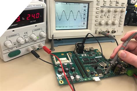
Functional Testing
Functional testing involves testing the PCB under real-world operating conditions to ensure it functions as intended. This can include testing the board’s power consumption, signal integrity, and overall performance.
| Advantages | Disadvantages |
|---|---|
| Tests the PCB under real-world conditions | Can be time-consuming |
| Can identify issues not detected by other methods | May require specialized test equipment |
| Ensures the PCB meets functional requirements | May not detect all defects |
Burn-In Testing
Burn-in testing involves subjecting the PCB to elevated temperatures and voltages for an extended period to identify any early-life failures or weak components. This method helps improve the reliability and longevity of the final product.
| Advantages | Disadvantages |
|---|---|
| Identifies early-life failures | Time-consuming |
| Improves product reliability | May not detect all defects |
| Can be combined with functional testing | Requires specialized test equipment |
X-Ray Inspection
X-ray inspection uses x-ray imaging to examine the internal structure of the PCB, including solder joints, vias, and component placement. This method can detect defects that are not visible on the surface, such as voids in solder joints or misaligned components.
| Advantages | Disadvantages |
|---|---|
| Can detect internal defects | High initial cost |
| Non-destructive testing | Requires specialized equipment and training |
| Can be automated for high-volume production | May not detect all defects |
Thermal Imaging
Thermal imaging uses infrared cameras to detect hot spots and temperature variations on the PCB during operation. This method can identify issues such as overheating components, poor thermal design, and insufficient cooling.
| Advantages | Disadvantages |
|---|---|
| Can identify thermal issues | Requires specialized equipment |
| Non-destructive testing | May not detect all defects |
| Can be performed during functional testing | Limited to thermal-related issues |
3D Automated X-Ray Inspection (3D AXI)
3D AXI combines x-ray imaging with computer tomography (CT) to create a detailed 3D model of the PCB. This method can detect a wide range of defects, including voids, cracks, and misalignments, with high accuracy and repeatability.
| Advantages | Disadvantages |
|---|---|
| High accuracy and repeatability | High initial cost |
| Can detect a wide range of defects | Requires specialized equipment and training |
| Non-destructive testing | May be slower than other methods |
High-Potential (HiPot) Testing
HiPot Testing involves applying a high voltage to the PCB to test its insulation and dielectric strength. This method helps ensure the PCB can withstand the required voltage levels without breaking down or causing safety issues.
| Advantages | Disadvantages |
|---|---|
| Tests insulation and dielectric strength | Can be destructive |
| Helps ensure product safety | Requires specialized equipment |
| Can be automated for high-volume production | May not detect all defects |
Solderability Testing
Solderability testing evaluates the ability of component leads and PCB pads to be successfully soldered. This method helps ensure the quality and reliability of solder joints and can identify issues such as poor wetting, oxidation, or contamination.
| Advantages | Disadvantages |
|---|---|
| Ensures solder joint quality | Destructive testing |
| Can identify solderability issues | Limited to solder joint evaluation |
| Can be performed on individual components | May not detect all defects |
Microsectioning
Microsectioning involves cutting a cross-section of the PCB and examining it under a microscope to evaluate the quality of internal structures, such as vias, plated through-holes, and copper traces. This method provides a detailed view of the PCB’s internal structure and can help identify manufacturing defects or quality issues.
| Advantages | Disadvantages |
|---|---|
| Provides detailed view of internal structures | Destructive testing |
| Can identify manufacturing defects | Time-consuming |
| Helps ensure PCB Quality | Requires specialized equipment and expertise |
FAQ
1. What is the most common PCB testing method?
The most common PCB testing method is Automated Optical Inspection (AOI), as it is fast, efficient, and can detect a wide range of visible defects.
2. Can a single testing method detect all possible defects in a PCB?
No single testing method can detect all possible defects in a PCB. A combination of different testing methods is often required to ensure comprehensive coverage and detect various types of defects.
3. What is the difference between destructive and non-destructive testing methods?
Destructive testing methods, such as microsectioning and solderability testing, involve damaging or destroying the PCB or its components during the testing process. Non-destructive methods, such as AOI, X-ray inspection, and thermal imaging, do not damage the PCB and can be performed on the final product.
4. How do I choose the right testing methods for my PCB Assembly process?
The choice of testing methods depends on various factors, such as the complexity of the PCB, the required level of quality and reliability, production volume, and budget constraints. It is essential to consider the specific requirements of your project and consult with experienced professionals to develop an appropriate testing strategy.
5. Can PCB testing be automated for high-volume production?
Yes, many PCB testing methods, such as AOI, ICT, and 3D AXI, can be automated for high-volume production. Automated testing helps ensure consistency, accuracy, and efficiency in the manufacturing process, reducing the risk of defects and improving overall product quality.
In conclusion, PCB testing is a critical aspect of the PCB assembly process, ensuring the quality, reliability, and functionality of the final product. By employing a combination of effective testing methods, manufacturers can identify and address defects early in the production cycle, reducing costs and improving customer satisfaction. As PCB technology continues to evolve, it is essential for manufacturers to stay up-to-date with the latest testing methods and technologies to maintain a competitive edge in the industry.


Leave a Reply