Introduction to PCB Composition
Printed Circuit Boards (PCBs) are the backbone of modern electronics. These boards are used in almost every electronic device, from smartphones and laptops to medical equipment and aerospace systems. PCBs are composed of various materials that work together to create a functional and reliable circuit board. In this article, we will dive deep into the composition of PCB boards, exploring the different layers, materials, and components that make up these essential pieces of technology.
The Layers of a PCB
Substrate Layer
The substrate layer is the foundation of a PCB. It is typically made of a non-conductive material, such as fiberglass or epoxy resin. The most common substrate material is FR-4, which is a flame-retardant composite made of woven fiberglass cloth and epoxy resin. This layer provides the rigidity and stability needed for the PCB to function properly.
Copper Layer
The copper layer is where the electrical connections are made on the PCB. This layer is typically made of a thin sheet of copper that is laminated onto the substrate layer. The copper is then etched away to create the desired circuit pattern. PCBs can have one or more copper layers, depending on the complexity of the circuit design.
| Number of Copper Layers | PCB Type |
|---|---|
| 1 | Single-sided PCB |
| 2 | Double-sided PCB |
| 4+ | Multi-layer PCB |
Solder Mask Layer
The solder mask layer is a protective coating that is applied over the copper layer. This layer helps to prevent short circuits and oxidation of the copper traces. It also provides a surface for the silk screen layer to be printed on. The solder mask is typically green in color, but can also be found in other colors such as red, blue, or black.
Silk Screen Layer
The silk screen layer is the top layer of the PCB. This layer is used to print text, logos, and other identifying marks on the PCB. The silk screen is typically white in color, but can also be found in other colors such as black or yellow. This layer helps to make the PCB easier to assemble and troubleshoot.

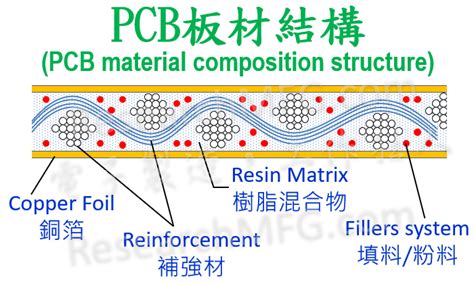
PCB Material Composition
FR-4
FR-4 is the most common substrate material used in PCBs. It is a composite material made of woven fiberglass cloth and epoxy resin. FR-4 has excellent mechanical and electrical properties, making it an ideal choice for PCBs. It has a high dielectric constant, which helps to reduce signal loss and crosstalk between traces.
Copper
Copper is the most common material used for the conductive layers in PCBs. It has excellent electrical conductivity and is relatively inexpensive compared to other conductive materials. The thickness of the copper layer can vary depending on the current carrying requirements of the circuit.
| Copper Thickness (oz) | Thickness (mm) |
|---|---|
| 0.5 | 0.0175 |
| 1 | 0.035 |
| 2 | 0.070 |
Solder Mask
The solder mask is typically made of a polymer material that is resistant to heat and chemicals. The most common solder mask materials are liquid photoimageable (LPI) and dry film photoimageable (DFPI). LPI is a liquid that is applied to the PCB and then cured using UV light. DFPI is a film that is laminated onto the PCB and then exposed to UV light to create the desired pattern.
Silk Screen
The silk screen is typically made of a polymer material that is resistant to abrasion and chemicals. The most common silk screen materials are epoxy and acrylic. The silk screen is applied to the PCB using a screen printing process, where the desired pattern is transferred onto the PCB using a stencil and a squeegee.

PCB Components
Surface Mount Components
Surface mount components are components that are mounted directly onto the surface of the PCB. These components are typically smaller than through-hole components and are used in high-density circuit designs. Some common surface mount components include:
- Resistors
- Capacitors
- Inductors
- Integrated Circuits (ICs)
Through-Hole Components
Through-hole components are components that are inserted into holes drilled in the PCB and soldered onto the opposite side. These components are typically larger than surface mount components and are used in lower-density circuit designs. Some common through-hole components include:
- Connectors
- Switches
- LEDs
- Transformers

PCB Assembly Process
Solder Paste Application
The first step in the PCB assembly process is to apply solder paste to the pads on the PCB. Solder paste is a mixture of tiny solder balls and flux that helps to create a strong mechanical and electrical connection between the components and the PCB. The solder paste is typically applied using a stencil and a squeegee.
Component Placement
Once the solder paste has been applied, the components are placed onto the PCB using a pick-and-place machine. This machine uses a vacuum nozzle to pick up the components and place them onto the PCB with high precision. The components are typically placed according to a computer-generated placement file that specifies the location and orientation of each component.
Reflow Soldering
After the components have been placed, the PCB is sent through a reflow oven. The reflow oven heats the PCB and the components to a temperature that melts the solder paste, creating a strong mechanical and electrical connection between the components and the PCB. The reflow process typically follows a specific temperature profile that is designed to minimize thermal stress on the components.
Inspection and Testing
Once the PCB has been assembled, it is inspected and tested to ensure that it meets the required specifications. This can include visual inspection, electrical testing, and functional testing. Any defects or issues that are found during the inspection and testing process are corrected before the PCB is shipped to the customer.
Frequently Asked Questions (FAQ)
What is the difference between a single-sided and double-sided PCB?
A single-sided PCB has copper traces on only one side of the substrate, while a double-sided PCB has copper traces on both sides of the substrate. Double-sided PCBs offer more routing options and can accommodate more components than single-sided PCBs.
What is the purpose of the solder mask layer on a PCB?
The solder mask layer serves several purposes on a PCB. It helps to prevent short circuits and oxidation of the copper traces, provides a surface for the silk screen layer to be printed on, and helps to protect the PCB from environmental factors such as moisture and dust.
Can a PCB have more than two copper layers?
Yes, PCBs can have more than two copper layers. These are known as multi-layer PCBs and can have four or more copper layers. Multi-layer PCBs are used in complex circuit designs that require a high degree of routing density and signal integrity.
What is the difference between surface mount and through-hole components?
Surface mount components are mounted directly onto the surface of the PCB, while through-hole components are inserted into holes drilled in the PCB and soldered onto the opposite side. Surface mount components are typically smaller and used in high-density circuit designs, while through-hole components are larger and used in lower-density designs.
How are PCBs tested to ensure they meet the required specifications?
PCBs are tested using a variety of methods to ensure they meet the required specifications. This can include visual inspection to check for defects or issues with the assembly process, electrical testing to verify that the PCB functions as intended, and functional testing to ensure that the PCB performs as expected in the final product.
Conclusion
PCBs are complex assemblies that are composed of various materials and components. Understanding the composition of a PCB is essential for anyone involved in the design, manufacture, or use of electronic devices. By exploring the different layers, materials, and components that make up a PCB, we can gain a deeper appreciation for the technology that powers our modern world. From the substrate layer that provides the foundation for the PCB, to the copper traces that carry electrical signals, to the components that perform specific functions, every aspect of a PCB plays a crucial role in creating a functional and reliable electronic device. As technology continues to advance, the composition of PCBs will undoubtedly evolve to meet the demands of new and innovative applications.


Leave a Reply