The Importance of PCB Etching
PCB etching is essential for creating the intricate patterns of copper traces that allow electronic components to communicate with each other. Without proper etching, a PCB would not function as intended, leading to device failures and potential safety hazards.
Accurate and precise etching ensures:
- Reliable electrical connections
- Optimal signal integrity
- Reduced electromagnetic interference (EMI)
- Improved overall performance of the electronic device
The PCB Etching Process
The PCB etching process typically involves the following steps:
- PCB Design
- Copper Cladding
- Applying Photoresist
- Exposure
- Development
- Etching
- Stripping and Cleaning
1. PCB Design
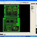
Before etching can begin, the PCB design must be created using specialized software. The design includes the placement of components and the routing of copper traces. This design is then used to create a photomask, which is a template for the etching process.
2. Copper Cladding
The starting material for a PCB is a substrate, typically made of fiberglass or epoxy, coated with a thin layer of copper on one or both sides. This copper layer will be selectively removed during the etching process to create the desired circuit pattern.
3. Applying Photoresist
A photoresist, a light-sensitive material, is applied to the copper-clad PCB. The photoresist can be applied using various methods, such as:
- Spin coating
- Dry film lamination
- Screen printing
The choice of application method depends on factors such as the desired resolution, production volume, and cost.
4. Exposure
The PCB with the applied photoresist is then exposed to UV light through the photomask. The photomask contains the circuit pattern and blocks UV light from reaching certain areas of the photoresist. Exposure to UV light causes a chemical change in the photoresist, making it either more soluble (positive photoresist) or less soluble (negative photoresist) in the developer solution.
5. Development
After exposure, the PCB is immersed in a developer solution. For positive photoresists, the exposed areas become soluble and are removed by the developer, revealing the copper layer underneath. For negative photoresists, the unexposed areas are soluble and removed, leaving the exposed photoresist to protect the copper during etching.
6. Etching
The developed PCB is then placed in an etching solution, which selectively removes the copper not protected by the photoresist. The most common etching solutions are:
- Ferric Chloride (FeCl3)
- Cupric Chloride (CuCl2)
- Alkaline Etchants (e.g., Sodium Persulfate)
The etching process can be performed using various methods, such as:
- Immersion Etching: The PCB is submerged in the etching solution, and the copper is removed through a chemical reaction.
- Spray Etching: The etching solution is sprayed onto the PCB surface, allowing for more uniform etching and better control over the etch rate.
The choice of etching method and solution depends on factors such as the desired etch rate, feature size, and environmental considerations.
7. Stripping and Cleaning
After etching, the remaining photoresist is stripped from the PCB using a solvent or an alkaline solution. The PCB is then thoroughly cleaned to remove any residues from the etching and stripping processes. The result is a PCB with the desired copper pattern, ready for further processing, such as drilling, plating, and component assembly.
Types of PCB Etching
There are two main types of PCB etching: subtractive and additive.
Subtractive Etching
Subtractive etching is the most common method and involves removing copper from a fully copper-clad PCB. This process follows the steps outlined in the previous section, with the photoresist acting as a mask to protect the desired copper areas during etching.
Advantages of subtractive etching:
– Well-established and widely used process
– Suitable for high-volume production
– Allows for the creation of fine features and high-density designs
Disadvantages of subtractive etching:
– Generates waste in the form of etched copper and spent etching solutions
– Requires careful control of the etching process to ensure consistent results
– May have limitations in terms of minimum feature size and spacing
Additive Etching
Additive etching, also known as pattern plating, involves selectively depositing copper onto a bare PCB substrate. The process typically involves the following steps:
- A thin layer of copper is deposited onto the entire PCB substrate using methods such as electroless plating or sputtering.
- A photoresist is applied and exposed through a photomask, as in the subtractive process.
- The exposed photoresist is developed, revealing the areas where copper should be deposited.
- Additional copper is electroplated onto the exposed areas, building up the desired thickness.
- The remaining photoresist is stripped, and the thin initial copper layer is etched away, leaving only the electroplated copper pattern.
Advantages of additive etching:
– Reduces waste by minimizing the amount of copper removed
– Allows for the creation of finer features and higher-density designs
– Enables the use of alternative substrate materials, such as flexible polymers
Disadvantages of additive etching:
– More complex process compared to subtractive etching
– May require specialized equipment and materials
– Limited adoption in high-volume production due to higher costs and longer processing times

Factors Affecting PCB Etching Quality
Several factors can influence the quality and consistency of PCB etching:
-
Photoresist Quality: The resolution, adhesion, and thickness of the photoresist can affect the accuracy and sharpness of the etched features.
-
Exposure and Development: Proper exposure time and development of the photoresist are crucial for creating a clean and accurate pattern for etching.
-
Etching Solution: The type, concentration, and temperature of the etching solution can affect the etch rate and the quality of the etched features.
-
Agitation: Adequate agitation of the etching solution ensures uniform etching and helps prevent undercut or overetching.
-
Etch Rate Control: Maintaining a consistent etch rate is essential for achieving the desired feature sizes and preventing defects such as overetching or incomplete etching.
-
Substrate Quality: The surface finish, thickness, and uniformity of the copper-clad substrate can impact the etching process and the final PCB Quality.
Proper control and optimization of these factors are essential for achieving high-quality PCB etching results.
PCB Etching Defects and Troubleshooting
Despite careful process control, various defects can occur during PCB etching. Some common defects and their potential causes include:
- Underetching: Insufficient removal of copper, leading to shorts or unintended connections.
-
Causes: Weak etching solution, low temperature, insufficient etching time, or poor agitation.
-
Overetching: Excessive removal of copper, resulting in broken or thinned traces.
-
Causes: Overly aggressive etching solution, high temperature, prolonged etching time, or excessive agitation.
-
Photoresist Adhesion Issues: Poor adhesion of the photoresist can lead to unintended etching or incomplete protection of copper areas.
-
Causes: Inadequate surface cleaning, incompatible photoresist, improper application, or insufficient drying time.
-
Undercutting: Etching of copper underneath the photoresist, resulting in narrower or damaged traces.
- Causes: Overly aggressive etching solution, high temperature, or prolonged etching time.
Troubleshooting PCB etching defects involves systematically analyzing the process parameters and identifying the root cause of the issue. This may require adjustments to the etching solution, exposure and development times, or process temperature, as well as ensuring proper surface preparation and photoresist application.
Environmental and Safety Considerations in PCB Etching
PCB etching involves the use of chemicals that can pose environmental and safety risks if not handled properly. Some key considerations include:
-
Proper Ventilation: Etching processes can generate fumes and vapors that may be harmful if inhaled. Adequate ventilation and fume extraction systems are essential to maintain a safe working environment.
-
Personal Protective Equipment (PPE): Workers involved in PCB etching should wear appropriate PPE, such as gloves, safety glasses, and protective clothing, to minimize exposure to chemicals.
-
Waste Management: Etching solutions and rinse waters containing dissolved metals and chemicals must be properly treated and disposed of in accordance with local environmental regulations. This may involve neutralization, precipitation, or other methods to remove harmful substances before discharge.
-
Chemical Storage and Handling: Etching chemicals should be stored in appropriate containers, labeled clearly, and kept in a secure, well-ventilated area. Proper handling procedures, including spill prevention and response plans, should be in place.
-
Regulatory Compliance: PCB manufacturers must comply with various environmental and occupational health and safety regulations, such as the Restriction of Hazardous Substances (RoHS) directive and the Registration, Evaluation, Authorization, and Restriction of Chemicals (REACH) regulation.
By implementing proper safety measures and adhering to environmental best practices, PCB manufacturers can minimize the risks associated with the etching process and ensure a safe and sustainable production environment.
Advances in PCB Etching Technology
As the demand for smaller, more complex, and high-performance electronic devices continues to grow, PCB etching technology must evolve to keep pace. Some recent advances and trends in PCB etching include:
-
Direct Imaging (DI): DI systems use high-resolution laser or LED light sources to directly expose the photoresist, eliminating the need for traditional photomasks. This allows for faster processing, improved accuracy, and the ability to create finer features.
-
Inkjet Printing: Inkjet printing technology can be used to selectively deposit etch-resistant materials onto the PCB substrate, creating a pattern for etching. This approach offers the potential for rapid prototyping and customization of PCBs.
-
Plasma Etching: Plasma etching uses a high-energy plasma to remove copper from the PCB surface. This method offers the potential for anisotropic etching, allowing for the creation of vertical sidewalls and improved feature resolution.
-
Laser Etching: Laser etching uses a high-powered laser to directly remove copper from the PCB substrate. This method offers high precision, speed, and the ability to create fine features without the need for photoresists or etching solutions.
-
Environmentally Friendly Etchants: Researchers are developing new etching solutions that are less toxic and more environmentally benign compared to traditional etchants. These include organic acids, such as citric acid, and hydrogen peroxide-based solutions.
As PCB etching technology continues to advance, manufacturers will be able to produce smaller, more complex, and higher-performance PCBs while reducing environmental impact and improving process efficiency.
Frequently Asked Questions (FAQ)
-
What is the difference between PCB etching and PCB Milling?
PCB etching is a chemical process that selectively removes copper from a PCB substrate to create the desired circuit pattern. PCB milling, on the other hand, is a mechanical process that uses a rotating cutting tool to remove copper and substrate material to create the circuit pattern. Etching is generally used for high-volume production and can create finer features, while milling is often used for prototyping and low-volume production. -
Can I etch my own PCBs at home?
Yes, it is possible to etch PCBs at home using a simplified process and readily available materials. However, home etching may not yield the same quality and consistency as professional PCB etching, and it is important to follow proper safety precautions when handling chemicals. For best results and safety, it is recommended to use professional PCB fabrication services. -
What is the minimum feature size that can be achieved with PCB etching?
The minimum feature size achievable with PCB etching depends on various factors, such as the photoresist resolution, etching method, and process control. Conventional subtractive etching can typically achieve feature sizes down to around 100 μm (4 mil). Advanced etching techniques, such as plasma etching or laser etching, can achieve even smaller feature sizes, down to a few microns. -
How do I choose the right etching solution for my PCB?
The choice of etching solution depends on factors such as the desired etch rate, feature size, substrate material, and environmental considerations. Ferric chloride and cupric chloride are widely used for their relatively low cost and good performance. Alkaline etchants, such as sodium persulfate, offer a more environmentally friendly alternative. It is important to consider the compatibility of the etching solution with the photoresist and the substrate material, as well as the safety and disposal requirements. -
What can I do to improve the quality and consistency of my PCB etching process?
To improve the quality and consistency of your PCB etching process, consider the following: - Ensure proper surface preparation and cleaning of the PCB substrate before applying the photoresist.
- Use high-quality photoresists and optimize the exposure and development process for sharp and accurate pattern transfer.
- Control the etching solution temperature, concentration, and agitation to maintain a consistent etch rate and prevent defects.
- Regularly monitor and maintain the etching equipment and solutions to ensure optimal performance.
- Implement quality control measures, such as visual inspection and electrical testing, to identify and address any issues promptly.
By understanding the fundamentals of PCB etching, selecting the appropriate methods and materials, and continuously optimizing the process, manufacturers can produce high-quality PCBs that meet the evolving demands of the electronics industry.
Here are two tables to summarize key information from the article:
| PCB Etching Process Steps | Description |
|---|---|
| 1. PCB Design | Create circuit pattern using software |
| 2. Copper Cladding | PCB substrate coated with copper layer |
| 3. Applying Photoresist | Light-sensitive material applied to copper |
| 4. Exposure | UV light exposure through photomask |
| 5. Development | Removal of soluble photoresist areas |
| 6. Etching | Removal of unprotected copper using etchant |
| 7. Stripping and Cleaning | Removal of remaining photoresist and cleaning |
| Types of PCB Etching | Advantages | Disadvantages |
|---|---|---|
| Subtractive Etching | – Well-established process – Suitable for high-volume production – Allows for fine features and high-density designs |
– Generates waste – Requires careful process control – May have limitations in feature size and spacing |
| Additive Etching | – Reduces waste – Allows for finer features and higher-density designs – Enables use of alternative substrate materials |
– More complex process – May require specialized equipment and materials – Limited adoption in high-volume production |
Leave a Reply