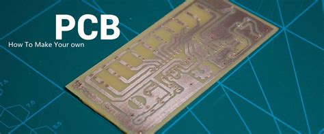
What is a PCB?
A Printed Circuit Board, or PCB, is a fundamental component in modern electronic devices. It is a flat board made of insulating material, typically fiberglass or composite epoxy, with conductive pathways etched or printed onto its surface. These pathways, also known as traces, connect various electronic components such as resistors, capacitors, and integrated circuits (ICs) to form a complete electrical circuit.
PCBs provide a compact and organized way to assemble electronic circuits, replacing the need for complex wiring and soldering of individual components. They are essential in the manufacturing of electronic devices, ranging from simple consumer gadgets to advanced industrial equipment and aerospace systems.
Key Components of a PCB
- Substrate: The base material of the PCB, usually made of fiberglass or composite epoxy.
- Copper Layers: Thin sheets of copper laminated onto the substrate, forming the conductive pathways.
- Solder Mask: A protective layer applied over the copper traces to prevent short circuits and provide insulation.
- Silkscreen: A printed layer on top of the solder mask that displays component labels, logos, and other information.
- Vias: Small holes drilled through the PCB to connect traces on different layers.
- Pads: Exposed areas of copper where components are soldered onto the board.
Types of PCBs
PCBs can be classified based on the number of conductive layers and their manufacturing process. The most common types include:
1. Single-Layer PCBs
Single-layer PCBs, also known as Single-Sided PCBs, have conductive traces on only one side of the substrate. They are the simplest and most cost-effective type of PCB, suitable for basic electronic circuits with low component density.
2. Double-Layer PCBs
Double-layer PCBs, or double-sided PCBs, have conductive traces on both sides of the substrate. The two layers are connected using vias, allowing for more complex circuits and higher component density compared to single-layer PCBs.
3. Multi-Layer PCBs
Multi-layer PCBs consist of three or more conductive layers separated by insulating layers. They offer the highest component density and are used in advanced electronic devices that require compact and complex circuitry. Multi-layer PCBs are more expensive to manufacture due to their intricate design and fabrication process.
4. Flexible PCBs
Flexible PCBs, or flex PCBs, are made using a flexible substrate material such as polyimide. They can bend and conform to various shapes, making them ideal for applications where space is limited or the device requires a non-planar design.
5. Rigid-Flex PCBs
Rigid-flex PCBs combine the features of both rigid and flexible PCBs. They consist of rigid sections connected by flexible sections, allowing for three-dimensional designs and improved reliability in applications that require both stability and flexibility.

PCB Manufacturing Process
The manufacturing of PCBs involves several steps, each requiring precision and adherence to industry standards. The general process includes:
- Design: The PCB layout is designed using specialized software, such as Altium Designer or Eagle CAD.
- Printing: The designed layout is printed onto a photosensitive film or directly onto the copper-clad substrate.
- Etching: The exposed copper is chemically etched away, leaving only the desired conductive traces.
- Drilling: Holes are drilled through the board for component leads and vias.
- Plating: The holes are plated with copper to ensure proper electrical connectivity between layers.
- Solder Mask Application: A protective solder mask is applied to the board, exposing only the areas where components will be soldered.
- Silkscreen Printing: Labels, logos, and other information are printed onto the solder mask using silkscreen printing.
- Surface Finish: A surface finish, such as HASL (Hot Air Solder Leveling) or ENIG (Electroless Nickel Immersion Gold), is applied to the exposed copper to prevent oxidation and improve solderability.
- Electrical Testing: The completed PCB undergoes electrical testing to ensure proper functionality and adherence to specifications.
| Step | Process | Description |
|---|---|---|
| 1 | Design | PCB layout is designed using specialized software |
| 2 | Printing | Layout is printed onto photosensitive film or copper-clad substrate |
| 3 | Etching | Exposed copper is chemically etched away |
| 4 | Drilling | Holes are drilled for component leads and vias |
| 5 | Plating | Holes are plated with copper for electrical connectivity |
| 6 | Solder Mask Application | Protective solder mask is applied, exposing areas for soldering |
| 7 | Silkscreen Printing | Labels, logos, and other information are printed |
| 8 | Surface Finish | Surface finish is applied to prevent oxidation and improve solderability |
| 9 | Electrical Testing | PCB undergoes electrical testing for functionality and adherence to specifications |

PCB Design Considerations
When designing a PCB, several factors must be considered to ensure optimal performance, reliability, and manufacturability:
1. Component Placement
Components should be placed in a logical and organized manner, minimizing the distance between connected components to reduce signal integrity issues and electromagnetic interference (EMI).
2. Trace Width and Spacing
The width and spacing of traces should be carefully calculated based on the current carrying capacity and the required impedance. Proper trace sizing helps prevent signal integrity issues and ensures reliable operation.
3. Power and Ground Planes
Dedicated power and ground planes should be used to provide a low-impedance path for power distribution and reduce noise. These planes also help to minimize EMI and improve signal integrity.
4. Thermal Management
Adequate thermal management is crucial for PCBs with high-power components. Proper heat dissipation can be achieved through the use of heatsinks, thermal vias, and appropriate component placement.
5. Signal Integrity
Signal integrity must be maintained by minimizing crosstalk, reflections, and other signal distortions. This can be achieved through proper trace routing, impedance matching, and the use of ground planes and shielding.
6. Manufacturing Constraints
The PCB design must adhere to the capabilities and constraints of the chosen manufacturing process. This includes minimum trace width and spacing, hole sizes, and clearances, among other factors.

Applications of PCBs
PCBs are used in a wide range of electronic devices and systems, including:
- Consumer Electronics: Smartphones, tablets, laptops, televisions, and home appliances.
- Automotive Electronics: Engine control units, infotainment systems, and advanced driver assistance systems (ADAS).
- Medical Devices: Diagnostic equipment, monitoring systems, and implantable devices.
- Industrial Equipment: Process control systems, automation equipment, and power electronics.
- Aerospace and Defense: Avionics, communication systems, and radar equipment.
- IoT Devices: Sensors, actuators, and communication modules for smart homes, wearables, and industrial IoT applications.
Future of PCBs
As electronic devices continue to evolve and become more complex, PCB technology must adapt to meet new challenges and demands. Some of the emerging trends in PCB design and manufacturing include:
1. High-Density Interconnect (HDI) PCBs
HDI PCBs feature finer traces, smaller vias, and higher component density, enabling the development of more compact and powerful electronic devices.
2. Embedded Components
Embedding components such as resistors, capacitors, and ICs within the PCB substrate can further reduce the size and improve the performance of electronic devices.
3. 3D Printing
Additive manufacturing techniques, such as 3D printing, are being explored for the fabrication of PCBs, offering greater design flexibility and faster prototyping.
4. Advanced Materials
New substrate materials, such as high-frequency laminates and ceramic-based substrates, are being developed to meet the demands of high-speed and high-temperature applications.
5. Environmental Sustainability
There is a growing focus on developing environmentally friendly PCB manufacturing processes and materials, such as halogen-free laminates and lead-free solders, to reduce the environmental impact of electronic waste.
Frequently Asked Questions (FAQ)
1. What is the difference between a PCB and a breadboard?
A breadboard is a temporary prototyping tool used to build and test electronic circuits without the need for soldering. PCBs, on the other hand, are permanent boards that provide a more reliable and compact solution for electronic circuits.
2. Can PCBs be repaired?
Yes, PCBs can be repaired, but the complexity and success of the repair depend on the extent of the damage and the type of components involved. Common repair techniques include soldering, trace repair, and component replacement.
3. How long do PCBs last?
The lifespan of a PCB depends on various factors, such as the quality of materials, manufacturing process, and operating environment. With proper design and maintenance, PCBs can last for several decades in normal operating conditions.
4. What is the typical turnaround time for PCB manufacturing?
The turnaround time for PCB manufacturing varies depending on the complexity of the design, the chosen manufacturing process, and the manufacturer’s workload. Simple PCBs can be produced within a few days, while complex multi-layer boards may take several weeks.
5. Are PCBs recyclable?
Yes, PCBs can be recycled to recover valuable materials such as copper, gold, and other metals. However, the recycling process is complex and requires specialized facilities to ensure the safe and environmentally friendly extraction of these materials.
In conclusion, PCBs are essential components in modern electronic devices, providing a compact and reliable platform for electrical circuits. Understanding the types, manufacturing process, and design considerations of PCBs is crucial for the development of effective and efficient electronic products. As technology continues to advance, PCB technology will evolve to meet the ever-increasing demands for performance, miniaturization, and sustainability in the electronics industry.


Leave a Reply