
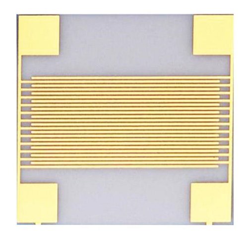
| Invented height term | Nominal | Allowed deviation |
|---|---|---|
| Ceramic | 500 µm | ±10 µm |
| Top metal | 4 µm | ±1 µm |
| Final attachment layer | 8 µm | ±3 µm |
| Die thickness | 100 µm | ±5 µm |
| Optical offset | 3 µm | ±1 µm |
| Defined total | 615 µm | ±20 µm worst case |
Start at the optical interface and work backward
A ceramic laser diode submount is more than a small thermally conductive rectangle. Its dimensions and metallization help establish where the attached device sits relative to the surrounding optical assembly. Begin the drawing with that functional relationship: which physical surface or fiducial defines the reference, which direction is critical, and what must remain accessible after attachment. The laser submount guide describes common construction choices. The drawing task is to convert the chosen construction into requirements that the substrate maker, die-attach team and optical assembly team can all measure without substituting different datums or assuming that nominal substrate thickness is the complete alignment specification.
Define whether the delivery is bare, metallized or solder coated
A procurement drawing must identify the delivered state. A bare ceramic, a metallized submount and a part with a patterned solder deposit have different dimensions and inspection needs. State which layers are included in every thickness callout and which will be added by the customer. ATP describes submounts with controlled substrate and metal thicknesses and pre-deposited patterned gold-tin. That is an example of an integrated supplied construction, not a reason to omit its individual interfaces from the drawing. If the supplier provides more than one deposition route, specify the approved route or define the evidence required to establish equivalence for the intended assembly.
Create a datum chain that survives assembly
Choose references that remain meaningful through receiving inspection, die placement and installation into the optical housing. An edge that is easy to locate under a microscope may be a poor height datum if the finished part rests on a different surface. Similarly, a fiducial used for lateral placement does not by itself define the vertical position of the emitting region. Show the mounting orientation and relate the relevant features to a consistent datum system. Include any keepout needed for the fixture or optical path. A clear datum chain reduces the risk that each supplier reports a good measurement while the completed assembly is misaligned because the measurements describe different relationships.
Worked height stack: count every contributing layer
Consider an invented vertical stack measured from a seating reference to an optical reference on the attached device. Assume five hundred micrometers of ceramic, four micrometers of top metallization, eight micrometers of final attachment layer, one hundred micrometers through the die and a further three-micrometer optical offset. The nominal sum is 615 micrometers. The example deliberately defines the signs and reference locations; a real device may require a different chain. If the final optical reference is measured directly from a finished surface, do not add a layer that is already included in that measurement. Draw the chain before performing arithmetic so that every term represents a distinct physical distance.
Allocate tolerances according to the complete stack
Suppose the five invented stack terms have symmetric allowed deviations of ten, one, three, five and one micrometers respectively. A conservative worst-case sum gives a total allowed deviation of twenty micrometers, assuming all deviations can align in the unfavorable direction. Tightening the ceramic term from ten to five micrometers reduces that total to fifteen micrometers; it does not eliminate the contribution from die thickness or the final attachment layer. These values are not supplier capabilities. They illustrate how to decide whether a requested ceramic tolerance addresses the actual alignment problem. A statistical combination requires justified distributions and dependencies, rather than replacing the worst-case sum with a smaller number by default.
Distinguish deposited solder thickness from the final joint
The as-supplied thickness of a solder pattern is not necessarily the final separation between die and submount after assembly. Wetting geometry, material redistribution, the die surface and the attachment process can affect that final state. Specify the deposited layer for substrate acceptance and the assembled bond line for assembly acceptance as separate requirements when both matter. Do not claim that controlling one guarantees the other. The height budget should use the final joint term that has been demonstrated for the selected assembly process. If that term remains uncertain, resolve it with representative assemblies before demanding an unnecessarily tight tolerance from the ceramic supplier.
Specify the metallization system as a sequence
A note such as gold finish leaves important questions unanswered. Identify the approved metal sequence, which surface it covers, the controlled thicknesses and the purpose of each functional region. The die landing, wire-bond pad and backside attachment surface may have different requirements. If a substitution is proposed, review its compatibility with all later joining operations. The drawing should also distinguish an intentionally conductive backside from an isolated backside. A ceramic body does not make the complete part electrically isolated if a via or edge wrap connects the two faces. Relate those conductive features to a net definition or an explicit continuity requirement.
Treat gold-tin composition and die backside metal together
Vishay's gold-tin substrate-mount literature explains that gold from a die's backside metallization can dissolve into the solder and alter the resulting alloy composition. The document discusses adjusting the supplied alloy for that situation. This is a specific reason to review the die backside stack together with the submount attachment material. Do not choose a solder composition from the substrate drawing while ignoring the material contributed by the die. Obtain the assembly supplier's qualified combination and process guidance. The published capability information is not a universal reflow recipe, and a nominal alloy label alone does not establish the behavior of the completed joint.
Dimension the landing, the solder pattern and the die separately
Show the conductive landing boundary, the deposited solder boundary and the maximum permitted die placement envelope as distinct features. Their relative offsets may determine whether an exposed region remains available for wire bonding or whether material can enter a protected optical area. Use the selected supplier's current process rules for feature size and registration, then check the assembled geometry with the actual die tolerances. Do not merge the three shapes into a single pad outline just because they look similar at the drawing scale. A separate overlay makes it easier to review a proposed die size change without accidentally approving a corresponding change to the solder pattern.
Define the facet and edge relationship explicitly
For an edge-emitting device, the relationship between the emitting facet and the submount edge can be a functional requirement. State whether the design requires a setback, a flush condition or a deliberate overhang, and identify who controls that dimension after placement. Include the allowed edge condition in the region that matters to the optical and attachment geometry. The laser machining guide provides background on defining a fabricated ceramic outline. Do not use a generic perimeter tolerance as a substitute for a critical local edge requirement. Conversely, avoid applying an optical-region requirement to every remote edge when that adds inspection effort without improving the assembly.
Evaluate seating and tilt at the relevant scale
Overall thickness alone does not determine the orientation of the attached device. The relationship between the seating surface and the local die landing can also matter. As a simple invented geometry example, an eight-micrometer height difference over a two-millimeter span corresponds to a slope of 0.004 and an angle of approximately 0.229 degrees. Extending that same straight line another five millimeters changes its height by twenty micrometers. This is a geometric illustration, not a prediction of laser beam pointing or optical coupling loss. Use the actual optical model to determine what surface orientation must be controlled and which measurement length is relevant.
Include the bond tool and optical keepout envelopes
A pad can satisfy its electrical dimensions while being inaccessible to the intended wire-bond tool. Coordinate the landing and bond-pad layout with the tool approach, neighboring components and the completed optical assembly. Reserve the space needed for inspection and handling as well as for the final device. Define whether markings, metallization or solder are allowed within each protected region. A drawing review should examine the assembly sequence, because a region accessible before die attachment may become obstructed afterward. Keep the geometric requirement tied to the chosen equipment or an agreed envelope so that future process changes can be reviewed deliberately.
State cleanliness and packaging requirements without inventing a shelf life
Agree on handling, packaging and storage conditions that preserve the supplied surfaces for the intended joining process. Identify which areas may be contacted by trays or handling tools and how the parts will be oriented. ATP's submount guidance discusses storage considerations for thin gold-tin layers, illustrating why storage should be addressed for the actual supplied construction. Do not convert that discussion into a universal shelf-life guarantee. Ask the supplier for the controlled packaging and storage instructions applicable to the ordered product, together with any reinspection needed after an agreed interval or a packaging breach. Record the lot and receiving date so that assembly behavior can be investigated later.
Choose first-article evidence that answers the drawing
A first-article report should show how each critical requirement was measured, not merely repeat the nominal dimensions in a table. Include the datum setup, measurement surface and the sampled locations for thickness or profile. Where attachment performance is part of qualification, use the actual die backside and the approved assembly process or explain the limitations of a representative test die. ATP describes lot reflow testing with defined test profiles; such a supplier test is useful evidence within its stated scope. It does not automatically validate every customer's device and assembly. Preserve the distinction between substrate acceptance and complete laser-module qualification.
Release an interface-controlled drawing package
The released package should include the mechanical drawing, conductor data, layer stack, attachment-material specification, relevant assembly envelopes and the inspection plan. Cross-reference the device revision that supplies the die dimensions and optical reference. State which changes require review by the optical and assembly teams, especially changes in substrate thickness, backside metal, solder pattern or datum features. The manufacturing specification guide can organize the records. A successful submount drawing controls the interfaces that determine the completed device position and joining behavior. It gives each supplier a clear responsibility while preserving the evidence needed to verify the combined stack after assembly.
Engineering example
All dimensions and tolerances in the worked stack and tilt examples are hypothetical. They are not capabilities of a named supplier, an optical alignment budget or a qualified solder process.
Before you release the design
- Define the delivered layer state and assembly datum chain.
- Separate deposited solder thickness from final bond-line height.
- Review die backside metal with the selected attachment alloy.
- Overlay landing, solder pattern and die placement envelopes.
- Match first-article measurements to the actual critical interfaces.
Sources and further technical reading
Manufacturer references support the material and process context. Worked examples and checklists are engineering guidance; they are not test results or supplier guarantees.