
| Illustrative check | Result | Boundary |
|---|---|---|
| (180−90)/2−20 micrometers | 25 micrometers | Not an acceptance limit |
| 1−0.05^(1/30) | Approximately 9.5% | Binomial independent-trial assumptions |
Specify a bonding system rather than a gold color
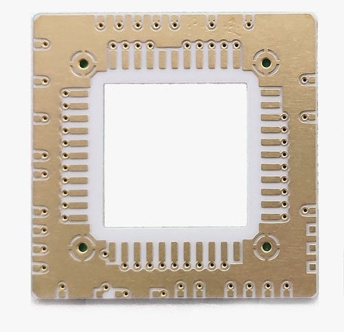
A ceramic circuit drawing that says gold finish does not tell an assembler whether the surface is suitable for the intended wire connection. The wire alloy, diameter, bonding method, underlying metals, surface condition and assembly history all influence the result. Begin with the electrical connection and manufacturing sequence, then choose a qualified pad construction. A finish selected for a solder joint can have a different purpose from a wire bonding finish even when both look gold. The ceramic wire bonding guide introduces layout considerations. This article focuses on documenting the finish selection so that purchasing, fabrication and assembly are working with the same interface.
Identify both ends of every wire
A wire connects two surfaces, and the substrate pad is only one of them. Record the die terminal metallization separately from the ceramic pad stack. Define which end receives a ball, stitch or wedge, as applicable to the selected process, rather than describing the entire assembly as gold bonding. Also identify ribbon connections separately from round wire. A process that works at the die end does not establish performance at the substrate end. Ask the assembly team to identify its limiting interface and the evidence required for that interface. Preserve these distinctions in test records so that a failed connection is assigned to the correct joint.
Use supplier constructions within their stated scope
Applied Thin-Film Products describes TiW/Au as a basic bondable thin-film construction and provides other stacks for combined attachment requirements. Its guidance distinguishes bondable and solderable gold and discusses special processing for some combinations. These are supplier-specific constructions, not permission to substitute any gold-bearing finish. Heraeus offers several gold wire purity families for different requirements, illustrating that the wire itself is also a selected product. Neither source establishes a universally successful pairing for a new ceramic circuit. Use the publications to frame a supplier discussion, then request written confirmation for the actual wire, pad structure and processing sequence under consideration.
Write the complete pad stack in a consistent direction
List the layers from ceramic toward the exposed bonding surface. Include the deposition or plating route where it affects the qualified construction, and distinguish nominal thickness from permitted limits. A gold thickness by itself leaves the adhesion and intermediate layers undefined. If the supplier uses a proprietary stack, reference a controlled supplier specification with an agreed revision and change notification requirement. The drawing can protect confidential process details while still identifying the purchased construction unambiguously. The surface finish overview helps separate finish families, but a general family name should not replace the controlled pad specification for a production assembly.
Keep bond pad and solder pad requirements separate
A circuit may need wire bonding, solder attachment and connector contact surfaces in nearby locations. Assign each pad its function on the drawing. Do not assume that increasing gold everywhere improves every attachment operation. Where the chosen supplier proposes selective metallization, define its boundaries and the registration tolerance between the selective layers and conductor pattern. Where one common stack is proposed, qualify every relevant attachment sequence with that common stack. Include exposed surfaces that remain unused during early assembly steps. A pad intended for later wire bonding may already have experienced cleaning, handling and heating during assembly of neighboring components.
Specify the condition at the moment of bonding
The finish arrives at the substrate receiving dock, but bonding occurs later. Draw a short process history from final fabrication cleaning through packaging, storage, unpacking, die attachment, cleaning and bonding. Identify the temperature exposure and chemicals at each stage using actual production instructions. Incoming bondability evidence on an untouched coupon may not represent a pad that has passed through the full sequence. Obtain test specimens at the intended bonding stage as well as at receipt when developing the process. This comparison helps distinguish an unsuitable supplied surface from a surface changed by the assembly route, without assuming either party caused the problem.
Control contamination without inventing a universal cleaning recipe
Handle bonding areas with fixtures and packaging that avoid direct contact with the functional surface. Define how operators recognize and segregate visibly contaminated parts, and specify the approved cleaning route with the assembler. Do not add an unqualified solvent wipe or aggressive treatment merely because it improves appearance. A visually clean surface and a bondable surface are different acceptance questions. If plasma or another surface treatment is used, record the equipment, process window and permitted delay before bonding. Demonstrate its effect on representative materials, including nearby die attach and printed features, rather than assuming a cleaning step is harmless to every construction.
Measure the footprint that must fit on the pad
Pad sizing should use the finished bonding footprint and positional variation, not only the undeformed wire diameter. For an illustrative straight placement check, suppose a finished pad is at least 180 micrometers wide, the maximum bond footprint is 90 micrometers wide and the placement center can deviate by 20 micrometers in either direction. The remaining minimum margin on the more crowded side is half the difference in widths minus that deviation: 25 micrometers. This is a geometric result for invented inputs, not an acceptable bonding margin. The assembler must establish the required margin and account for footprint orientation, edge quality and its actual process capability.
Check tool access and local support independently
A footprint may fit while the bonding tool cannot approach the location safely. Review the tool envelope against nearby die, walls, components and existing wires over the complete bonding sequence. Include substrate placement and height tolerances rather than checking only nominal top views. The supporting fixture also needs to represent the ceramic assembly during process development. A coupon held flat against a rigid surface may behave differently from a production tile supported around an opening. Review support beneath the bond region with the assembler and prevent fixture loading from becoming an unexamined source of substrate damage or inconsistent energy transfer.
Make qualification coupons representative
A useful coupon reproduces the interface being qualified. Specify ceramic grade and surface preparation, metal stack, final thickness limits, fabrication lot relationship and the preceding assembly exposures. Include the intended pad dimensions where small geometry could affect the bonding operation. A conveniently large test pad can conceal a placement or edge problem on the actual circuit. Conversely, a coupon designed only for geometry evaluation may not represent the production metallization lot. Record exactly what the coupon demonstrates and what remains to be checked on representative assemblies. Supplier sample success becomes useful evidence when its relationship to the purchased circuit is traceable.
Treat pull and shear results as different measurements
Bond tests should follow a defined method agreed with the assembler and product owner. Record the tested bond type, loading arrangement, tool position, speed, sample preparation and failure classification alongside the measured force. A pull test of a wire loop and a shear test of a bonded feature interrogate different geometries; their numbers should not be combined into one acceptance threshold. Preserve individual results and failure locations instead of reporting only the largest force or the batch average. A high measured force does not, by itself, identify which interface was sound or explain why another sample failed under a different loading configuration.
Separate development sampling from demonstrated reliability
A small process trial can reveal poor settings, but it does not prove a low field failure probability. Consider an illustrative statistical check with thirty independent, identically distributed trials and no failures. Under a simple binomial model, the one-sided upper failure probability at ninety-five percent confidence is one minus 0.05 raised to the power of one divided by thirty, approximately 9.5 percent. The assumptions are strong and often inappropriate for multiple bonds made on one shared coupon. The calculation explains why zero failures in a small trial should not be marketed as near-perfect reliability. Use a qualification plan matched to the product risks and population.
Evaluate the intended environment after assembly
Initial bonding success is only the start of the evidence. Define the product temperature history, mechanical loading, humidity exposure and enclosure conditions that are relevant to the application. Select qualification exposures and acceptance criteria through the responsible reliability process, with checks before and after exposure. A test program developed for one wire and pad combination should not automatically transfer to another combination because both use a ceramic base. Preserve the complete assembly configuration, including encapsulation or protection where used. Distinguish damage at the wire, bond interface, underlying film and ceramic so that corrective action addresses the observed mechanism rather than simply changing gold thickness.
Investigate failures in a structured order
When bonds fail, first verify that the samples match the approved drawing, wire product and assembly records. Compare the affected locations, fabrication lots and processing history with successful controls. Then examine the failure surfaces and the relationship between force results and failure classifications. Changing wire, pad finish, cleaning and machine settings simultaneously can produce a passing trial without identifying the reason. Where practical, use controlled comparisons that separate these factors while preserving a representative assembly. Retain failed samples and their orientation. A traceable failure investigation is more valuable than a finish substitution justified only by a favorable repeat test on a different specimen.
Qualify substitutions before purchasing them
Purchasing may receive an offer for an apparently equivalent gold finish, a different plating source or a replacement wire grade. Evaluate the proposed difference against the qualified interface description. A change to an intermediate layer, surface treatment, alloy or preceding heat exposure can fall outside the evidence supporting the original combination. Ask the supplier to identify the changed characteristics explicitly. Define which checks can demonstrate equivalence and which require assembly qualification. The material selection guide addresses the broader substrate decision; preserve the same change discipline when the ceramic stays constant but its bonding interface changes.
Release a drawing and evidence package together
The final specification should connect each pad function to its controlled metal stack, thickness limits, finished geometry and approved assembly route. Include packaging and storage requirements supported by the selected suppliers, rather than inventing a shelf life for all ceramic finishes. Reference the wire product, coupon relationship, qualification report and test methods with revision identifiers. Resolve disagreements about acceptable failure classifications before production starts. This package lets a fabricator quote the intended surface and lets an assembler reproduce the interface that was evaluated. A gold appearance or a generic bondable label alone cannot provide that level of control.
Engineering example
All example dimensions and trial counts are hypothetical. No pad stack, bonding margin, test force or qualification limit is prescribed.
Before you release the design
- Identify both bonded surfaces and the wire product.
- Specify the complete stack and preceding assembly exposures.
- Check finished footprint, tool access and support.
- Use representative coupons and defined failure classifications.
- Approve substitutions against the qualified configuration.
Sources and further technical reading
Manufacturer references support the material and process context. Worked examples and checklists are engineering guidance; they are not test results or supplier guarantees.