
| Invented model | Result | Scope |
|---|---|---|
| 3 mm lateral length,6 mm width,0.30 mm thickness, k390 W/m·K | 4.27 K/W | Isolated one-dimensional strip |
| Same strip at0.60 mm thickness | 2.14 K/W | No distributed heat exit |
| Source1 rise:1.8×10+0.30×6 | 19.8 K | Assumed linear coefficients |
| Source2 rise:0.30×10+2.2×6 | 16.2 K | Fixed thermal reference |
Copper geometry determines where heat can spread
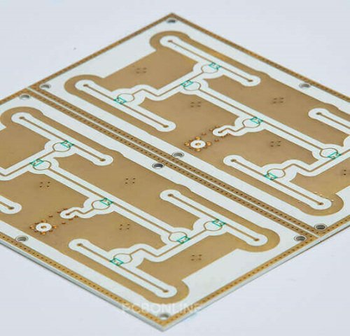
Copper on a ceramic substrate can distribute heat laterally as well as carry electrical current. Its usefulness depends on the connected shape available around the heat source and on where the heat can leave the assembly. A large amount of copper elsewhere on the tile does not necessarily help a die connected to a small isolated island. Begin with a map of the heat sources, copper regions, ceramic outline and lower cooling contact. The copper thickness guide introduces the broader construction tradeoffs. This article focuses on evaluating the spreading function without treating copper area or thickness as an automatic measure of complete thermal performance.
Separate heat spreading from heat rejection
Spreading redistributes heat within the structure; it does not remove energy from the system by itself. The redistributed heat still needs a path to the cooler, surrounding air or another defined exit. Increasing an upper copper area may produce little benefit if the lower contact remains restricted or the external cooling path dominates. Identify the temperature difference that the proposed copper change is intended to reduce. A cooler surface temperature and a lower junction temperature are not interchangeable observations. Keep the complete thermal path visible so that a local geometry improvement is evaluated in the context of the actual heat-rejection arrangement.
Recognize why thickness can have competing effects
Infineon's discussion of smart module design explains that thicker conducting layers can provide more spreading while also adding through-thickness path length. Which effect dominates depends on the geometry and heat-flow distribution. This is a reason to analyze the actual stack rather than assert that more copper always lowers thermal resistance. Rogers' AMB technology description likewise identifies thick copper as a heat-spreading feature within its substrate construction, not as a universal temperature guarantee. Treat supplier descriptions as context for a product-specific comparison. Keep source size, copper pattern, ceramic layer and cooling boundary fixed where possible when investigating a thickness change.
Use a simple lateral strip model to understand direction
For an invented isolated copper strip, assume heat flows only along a three-millimeter length through a six-millimeter width and a 0.30-millimeter thickness. With an assumed conductivity of 390 watts per meter kelvin, the one-dimensional resistance along the strip is approximately 4.27 kelvin per watt. Doubling thickness to 0.60 millimeters halves that lateral resistance to approximately 2.14 kelvin per watt. This is not the spreading resistance of a real ceramic board. The model deliberately excludes heat leaking into the ceramic along the strip, spatial spreading and contact effects. Its purpose is to show how thickness enters the conducting cross section for lateral flow.
Contrast the lateral model with through-thickness flow
For a uniform vertical path through a fixed area, resistance is proportional to the layer thickness rather than inversely proportional to it. Doubling copper thickness therefore doubles that layer term in the ideal vertical calculation, while halving the ideal lateral-strip term in the previous example. There is no contradiction because the direction and cross section differ. A real substrate combines these effects in a spatial field. Do not add the two illustrative resistances as though they were automatically two series elements in the actual assembly. Use them to understand the competing geometry relationships, then select a model that represents where the heat enters and leaves the copper.
Map islands and narrow connections before counting area
Electrical isolation divides many power layouts into separate copper regions. A narrow connection between a die landing and a remote copper area can restrict the thermal path, while an electrically isolated neighboring island is not a direct copper extension of that landing. Keep the actual connected geometry in the model. A spreadsheet using total copper coverage over the tile can hide those distinctions. Review neck widths, slots, rounded boundaries and holes that interrupt a potential lateral route. If a larger copper region requires a change to the circuit or insulation layout, treat that as a separate design decision rather than adding metal solely to improve a thermal picture.
Review source placement relative to the available spreading region
A source near the center of a broad island has a different available geometry from one close to a boundary or a narrow neck. Compare the intended die locations using the actual placement and landing dimensions. Include the source footprint and attachment layer rather than modeling the entire copper island as uniformly heated. If a placement change also alters bond-wire length or assembly access, preserve those constraints in the decision. A thermal model that ignores the product's electrical and manufacturing requirements can propose a layout that is impossible to build. The useful result is a feasible source arrangement with a demonstrated temperature benefit under the intended operating conditions.
Evaluate thermal coupling between neighboring sources
A copper region that spreads heat efficiently can also couple the temperatures of nearby devices. Infineon's module discussion explicitly considers interactions between multiple chips within a shared thermal stack. Evaluate the relevant combinations of source power rather than optimizing each die in isolation. A source that is cool when its neighbor is off may be limiting when both operate. Conversely, a geometry that reduces a local peak can change the heat reaching a temperature-sensitive component elsewhere. Record the source map and operating modes with the comparison. Thermal coupling is part of the design outcome, not an error to hide by reporting only the best single-device result.
Worked coupling example for a fixed linear model
Assume a hypothetical linear steady model with two sources measured relative to a fixed thermal reference. Let the temperature-rise coefficients be 1.8 kelvin per watt for source one's own power, 2.2 for source two's own power and 0.30 for each cross-coupling term. With ten watts at source one and six watts at source two, the modeled rises are 19.8 kelvin and 16.2 kelvin respectively. These coefficients are invented, not measured or simulated results. The example shows how neighbor power contributes to each temperature. Superposition requires the fixed-property and boundary assumptions of the linear model; it should not be applied without review to strongly temperature-dependent conditions.
Distinguish upper copper, lower copper and a separate baseplate
The upper conductor pattern, lower metallization and an attached baseplate can each distribute heat, but they occupy different locations in the path. A continuous lower layer cannot be substituted for the upper source-connected geometry without accounting for the ceramic between them. Similarly, a thick external baseplate has its own attachment and cooling interfaces. Draw each layer and define its material, thickness and contact area. When comparing a substrate with another construction, identify which spreading function moved and which interface was added or removed. This prevents a claimed benefit from being assigned to ceramic or copper thickness when the actual change was in the baseplate or mounting contact.
Keep mechanical and fabrication constraints in the copper review
Changing copper thickness or coverage can affect the manufacturability and mechanical behavior of the substrate. Review the supplier's finished geometry rules, registration and stack options along with the thermal result. A design that improves a thermal model but requires an unqualified metal-to-ceramic construction is not yet a production solution. Keep opposite-side copper, local pattern changes and the assembly support condition visible. If a prototype changes several of these at once, report the comparison as a combined construction change rather than isolating the credit to spreading. The manufacturer should confirm the feasible stack and the inspection basis before its performance is treated as an available design option.
Do not use a uniform contact where the real cooler is localized
The lower boundary can determine whether added copper area is useful. A model that holds the entire underside at one temperature may overstate the benefit of material extending beyond a limited mounting region. Represent the actual contact footprint, interface layer and relevant temperature variation, or explain why a simpler boundary is adequate for the decision. Compare a proposed copper change under the same boundary conditions. If the mounting arrangement changes too, separate its contribution where practical. The question is not merely how widely heat spreads across the board, but whether that distribution connects the source effectively to the available heat exit.
Use measurements that can distinguish spreading from other changes
A controlled experiment should keep source power, attachment quality, cooling condition and sensor method consistent while changing the intended copper variable. Measure the source-related temperature and selected surrounding locations where they help interpret the heat distribution. A cooler remote surface can indicate less heat reaching that location rather than better source cooling, so avoid judging the result from a single convenient point. Record the actual copper dimensions and assembly state of the specimens. If the measured improvement is comparable with uncertainty in power or contact condition, resolve those uncertainties before claiming that the copper change produced a reliable benefit.
Check transient behavior when the load changes quickly
Copper adds thermal mass as well as a conducting path. During a short or changing power event, stored energy and the time available for heat to reach different regions can affect the temperature response. A steady spreading comparison cannot by itself establish a transient peak. Use the relevant pulse duration, repetition and starting condition, with suitable material heat-capacity data and time resolution. If a reduced thermal network is used, validate it for the geometry and operating range of interest. Do not treat an observed slower warmup as proof of a lower steady thermal resistance; those observations can reflect different properties of the assembly.
Choose copper changes using a complete design comparison
The final comparison should include the required source temperatures, thermal coupling, electrical layout, feasible stack, attachment and cooling conditions. Record which quantities were calculated, measured or assumed, and preserve the operating cases that set the limits. A larger island or thicker layer may be worthwhile, but its benefit should be demonstrated against alternatives such as source placement, attachment improvement or a revised cooling contact. Copper heat spreading is a geometric and system property, not a single material number. A successful design identifies the path made better by the added metal and verifies that the complete assembly still meets its electrical, mechanical and manufacturing requirements.
Engineering example
The strip and coupling examples are hypothetical and are not actual board simulations. They illustrate directional conduction and neighboring-source interaction without prescribing a copper thickness.
Before you release the design
- Map the connected copper geometry and actual heat exits.
- Keep lateral spreading distinct from vertical layer resistance.
- Evaluate source location and neighboring power combinations.
- Use the real lower contact boundary.
- Verify the complete thermal, electrical and mechanical tradeoff.
Sources and further technical reading
Manufacturer references support the material and process context. Worked examples and checklists are engineering guidance; they are not test results or supplier guarantees.