
| Illustrative lateral removal per side | Protected width | Calculated top width |
|---|---|---|
| 0.08 mm | 1.20 mm | 1.04 mm |
| 0.10 mm | 1.20 mm | 1.00 mm |
| 0.12 mm | 1.20 mm | 0.96 mm |
Specify the finished feature before discussing compensation
For a DBC ceramic PCB, the conductor dimension needed by the circuit is not necessarily the dimension drawn in the production phototool. Etching removes exposed copper and can alter the conductor profile beneath the protective pattern. The supplier controls its compensation for the selected foil, chemistry and equipment. Your drawing should communicate the required finished geometry and the place where it is measured. Begin with the DBC process guide, then separate electrical conductor width, component landing area and the nearest-metal spacing into individually inspectable requirements.
Name the edge used by the dimension
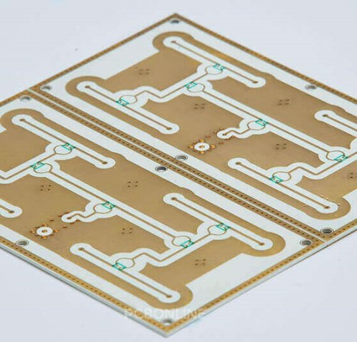
A thick etched conductor should be understood as a three-dimensional feature. Its edge at the outer copper surface may not coincide with the edge close to the ceramic. A top-view image can therefore answer a different question from a section through the conductor. Mark whether a critical width refers to the top landing surface, the base or an agreed measurement plane. For a gap, specify which two physical boundaries define the separation. Avoid a drawing that uses the word width for several different edge definitions without a section detail; a supplier can otherwise meet one interpretation while the assembled part fails another.
Treat the process profile as measured data
Do not assume a universal relation between copper thickness and lateral removal. A convenient geometric example can help calculate sensitivity, but it does not establish the actual profile for a supplier's process. Ask for the design rules applicable to the proposed copper thickness and finished surface condition. Request an explanation of tolerance, artwork compensation and inspection capability at the critical feature. If the supplier reports a typical result, determine what acceptance limit is being offered. The trace and space guide provides the broader layout context; use the controlled process agreement for production dimensions.
Worked sensitivity example for a landing pad
Suppose an illustrative process model starts with a protected width Wp of 1.20 mm and assumes lateral removal u at each side of the top edge. Within that deliberately simplified model, Wtop = Wp − 2u. At u = 0.08, 0.10 and 0.12 mm, top widths are 1.04, 1.00 and 0.96 mm. A device needing 1.00 mm of usable landing width has no positive dimensional allowance in the middle case. The example is not a prediction of DBC undercut: it shows that a 0.02 mm change on each side changes usable width by 0.04 mm. Ask the manufacturer to replace these illustrative inputs with its actual geometry and tolerances.
Add placement and attachment allowances separately
A finished pad width is not the whole attachment budget. The component, die or terminal has dimensional tolerance; its placement has error; the attachment process may require a usable border or a defined material boundary. For a centered rectangular case, a simple nominal side allowance is (Wpad − Wpart)/2. A hypothetical 1.20 mm finished pad and 1.00 mm part leave 0.10 mm per side before placement error and all tolerances are considered. If lateral placement can shift 0.07 mm, only 0.03 mm remains on the limiting side in this nominal calculation. Evaluate the actual tolerance stack rather than borrowing those numbers as a design rule.
Check current flow using an appropriate cross-section
A conductor whose section is not rectangular should not automatically be assigned area equal to its widest visible width times thickness. For a hypothetical trapezoid with parallel widths 0.80 and 1.00 mm and thickness 0.30 mm, geometric area is 0.30 × (0.80 + 1.00)/2 = 0.27 mm². Using 1.00 × 0.30 would overstate area by about 11.1%. This idealized geometry does not include finish, edge roughness or constrictions at transitions. The trace-resistance calculator can screen resistance assumptions, but a current rating requires temperature and boundary-condition evidence beyond a cross-sectional area calculation.
Review the thickness and spacing combination
Rogers publishes different typical conductor width and spacing entries for different copper thicknesses in its curamik data. That is useful evidence that a single feature rule should not be carried unchanged across every thickness. It is not permission to apply those typical values to an unrelated fabrication route or to treat them as electrical insulation distances. When thicker copper is proposed for lower resistance, recheck pad accessibility, edge definition, minimum gaps and the attachment layout. The copper-thickness guide helps organize that trade, while the supplier must confirm the achievable finished pattern.
Keep solder control features distinct from conductor gaps
Rogers describes functional areas for die attachment and interconnection, and discusses solder-control options including mask and structured copper surfaces. These features serve a process purpose; their names alone do not establish electrical separation. A groove that constrains attachment material is not automatically an isolation gap through the metal. Show the depth or construction of any such feature in the drawing, state what function it must provide, and identify its inspection method. Do not infer the connectivity of a structure from a photograph or from a top-view pattern without the relevant section information.
Close the loop with an approved drawing and inspection sample
Before ordering production, have both parties agree the final drawing revision, edge definitions, critical tolerances and any compensation responsibility. A supplier's corrected artwork should remain traceable to the customer requirement rather than silently becoming the only dimensional record. Review representative finished features using the agreed inspection approach and relate the findings to assembly trials. Record exceptions explicitly. Bring the outcome into the DFM release checklist so that a later copper-thickness or supplier change triggers a renewed review instead of inheriting assumptions from a different etching process.
Build a dimension chain from the actual functional surface
Start with the feature that must work after assembly and work backward toward fabrication. For a terminal landing, the functional requirement may be a minimum usable top surface over a defined length. For a current path, it may be a minimum conductor section at a narrow transition. For an isolation gap, the relevant condition may be the closest finished metal boundaries rather than a nominal artwork opening. These are separate requirements even when they lie beside each other. Draw a section through the critical location and label every measurement plane. If plating is applied after etching, state whether acceptance is before or after that finish. Record whether a dimensional limit includes the finish. A drawing with one clearly defined functional dimension is easier to manufacture than several apparently precise dimensions that conflict.
Distinguish nominal compensation from guaranteed output
A supplier may enlarge a protected feature in its production artwork to obtain the requested finished width. That compensated width is a process input, not a promise that every feature will lose exactly the same amount of metal. Ask how the supplier relates its artwork rules to the finished-part tolerance and how it handles unusually large pads, narrow necks and abrupt transitions. Do not add your own compensation to a drawing that the supplier will compensate again unless the responsibility is explicitly agreed. Keep customer design data and supplier production data separately identified. When a prototype fails a dimension, investigate which representation was actually used before altering the electrical design. Otherwise, an avoidable data-interpretation problem can become an unnecessary circuit redesign.
Calculate a worst-case usable border
Extend the illustrative attachment example by assigning a minimum finished pad width of 1.16 millimeters, a maximum part width of 1.02 millimeters and a maximum lateral placement offset of 0.04 millimeters. Under a centered rectangular model, the limiting side border is half the difference in widths minus the offset. The result is 0.03 millimeters. If the attachment process needs a larger border, the nominal pad size alone cannot show compliance. These numbers are invented for arithmetic demonstration and are not a recommendation for any package. Also check the orthogonal direction and any rotation error. A rectangular part rotated relative to a rectangular pad changes corner clearances, so the simple one-axis equation should not be used as a complete placement-envelope calculation.
Check resistance sensitivity without promising current capacity
For the hypothetical trapezoidal section, using an area of 0.27 square millimeters instead of 0.30 increases calculated resistance by a factor of 0.30 divided by 0.27 when resistivity and length are unchanged. That factor is approximately 1.111. At a fixed current, calculated resistive heating changes by the same factor because power is current squared times resistance. At a fixed voltage applied across the conductor, however, the electrical boundary is different; it is inappropriate to transfer the same heating conclusion without solving the circuit. Real operating temperature can also change resistivity. State the assumed electrical condition with the comparison. This is a geometric sensitivity calculation, not evidence that a conductor may safely carry a particular current or that its temperature rise will increase by exactly the same percentage.
Treat inspection images as measurements with a definition
A magnified top-view image may show a bright edge, a shadow or a finish boundary rather than the physical boundary intended by the drawing. Before accepting an automated measurement program, agree the edge-detection convention and check it on representative parts. Specify the location along the feature, since a rounded corner and a straight segment need not produce the same width. Keep the optical method separate from destructive cross-section measurements; the two methods may be useful for different questions. If cross sections are used during qualification, record their positions and orientation. A section that misses the narrowest location does not establish the minimum section everywhere along the conductor. Use the inspection plan to connect the sampled geometry to the actual functional risk.
Use coupons carefully when the product pattern is unusual
A process coupon can provide convenient access for measurement, but it should represent the feature being qualified. A long isolated line may not reproduce a dense array of large copper islands, and a coupon located elsewhere on a manufacturing panel may experience different local conditions. Ask the supplier which coupon features are intended to monitor general process stability and which directly represent product acceptance. Where a critical product feature can be measured nondestructively, compare coupon and product results during initial qualification. Preserve the distinction between monitoring a process and inspecting every critical feature. A passing coupon is valuable evidence only within the relationship that has been established; it should not silently replace a product requirement that was never included in the coupon design.
Review transitions and terminations, not just straight traces
The narrowest electrical section may occur at a pad neck, a corner or the end of a slot rather than in the middle of a nominally uniform trace. Mark these locations in the manufacturing review and ask how the finished geometry is represented in inspection. For attachment areas, consider the complete usable shape, including corner rounding and local interruptions. A pad can meet a centerline width while lacking a usable corner region needed by the component. Do not infer that every geometric discontinuity will cause a failure; instead identify which discontinuities intersect a current path, an attachment boundary or a defined spacing requirement. This keeps the review focused on functional geometry instead of accumulating dimensions that have no clear acceptance purpose.
Resolve an out-of-tolerance feature before broadening the limit
When a finished feature is smaller than requested, first establish that both parties measured the same physical boundary and revision. Check the associated assembly requirement and whether the discrepancy is systematic or limited to particular locations. A concession should identify the affected quantity and the evidence supporting its disposition. If the design can tolerate a changed dimension, revise the controlled requirement deliberately and reassess related tolerances. Do not simply change a nominal number so that the existing batch appears conforming while leaving the original functional requirement unchanged. Keep the supplier's production correction separate from the customer's design correction. This distinction makes the next order reproducible and prevents a temporary exception from becoming an undocumented permanent design rule.
Engineering example
The width table uses Wtop = Wp − 2u as a hypothetical sensitivity model. It does not prescribe phototool compensation, claim an etch factor or guarantee a DBC profile. Finished conductor sections and tolerances require supplier-specific evidence.
Before you release the design
- Identify the physical edge and measurement plane for each critical dimension.
- Separate artwork compensation from finished-part acceptance.
- Include component tolerance, placement and attachment allowances.
- Review conductor cross-section and electrical spacing independently.
- Reapprove the drawing when thickness, process or supplier changes.
Sources and further technical reading
Manufacturer references support the material and process context. Worked examples and checklists are engineering guidance; they are not test results or supplier guarantees.