
| Hypothetical calculation | Result | Interpretation |
|---|---|---|
| 1.8 V × 80 A − 72 W optical | 72 W heat | Same operating point and boundary |
| 200 microseconds × 100 Hz | 2% duty cycle | Pulse contribution averages 1.44 W |
| 0.0005/(170 × 0.00001) | 0.294 K/W | Uniform one-dimensional layer only |
| 2 ppm/K × 10 mm × 150 K | 3 micrometers | Free differential expansion, not stress |
Define the carrier within the laser assembly
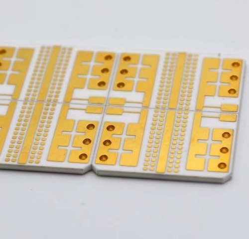
An aluminum nitride carrier for a high-power laser diode bar has to satisfy thermal, electrical, mechanical and optical requirements at the same time. Selecting a ceramic conductivity value is only one part of that decision. Identify the bar, its attachment joint, the patterned carrier, the lower attachment or contact, and the cooler before comparing materials. State whether the deliverable is a bare metallized tile, an attached bar or a complete aligned module. These boundaries determine who controls the interfaces and who can verify optical performance. The laser submount overview provides the broader product context; the bar-specific problem requires particular attention to temperature distribution and alignment along the emitting array.
Keep optical output separate from dissipated heat
The heat entering the carrier is not the advertised optical output power. Use electrical input and emitted optical power measured at the same operating point, with a boundary that identifies any other included losses. In a hypothetical bar operating at 1.8 volts and 80 amperes, electrical input is 144 watts. If optical output at that condition is 72 watts, the corresponding difference is 72 watts. This simple energy balance excludes driver losses and assumes the identified optical power leaves the bar boundary. It is an engineering example, not a specification for any cited product. Record the operating temperature and mode alongside the values because the balance can change with operating conditions.
Define continuous and pulsed conditions separately
A carrier assessed for continuous operation cannot be qualified for every pulsed condition by comparing average power alone. For an illustrative rectangular heat pulse of 72 watts lasting 200 microseconds at a repetition rate of 100 hertz, the duty cycle is two percent and the time-average pulse contribution is 1.44 watts. The instantaneous source still reaches 72 watts during the pulse. Include any heat generated between pulses and use the relevant transient thermal response to evaluate peak temperature. Coherent's conduction-cooled bar datasheet distinguishes continuous and quasi-continuous operating conditions and states a cold-plate reference. That is useful documentation practice; its ratings do not establish the limits of a different AlN carrier.
Request the actual ceramic grade and measurement conditions
Aluminum nitride is a material family with supplier-specific grades and properties. Request thermal conductivity information relevant to the intended temperature range, together with the thickness and finished geometry that will be supplied. Do not compare room-temperature typical values as if they were guaranteed complete-module performance. Kyocera identifies AlN as a thermally conductive laser submount material and offers configurable thin-film structures. That supports considering AlN for this function, but it does not certify a particular bar and cooler combination. The aluminum nitride material guide can organize the material questions before the design is converted into a controlled supplier drawing.
Use simple layer calculations only within their geometry
Consider a hypothetical uniform layer calculation using a ceramic thickness of 0.5 millimeters, conductivity of 170 watts per meter kelvin and a selected conduction area of 10 square millimeters. Dividing thickness by conductivity and area gives approximately 0.294 kelvin per watt. At 72 watts, that idealized layer would produce a temperature difference of about 21.2 kelvin. The calculation assumes one-dimensional flow through the stated area. A real laser bar, metal pattern, attachment joint and cooler do not necessarily preserve that area through the stack. Use the result to check units and sensitivity, not as a guaranteed junction-to-cooler resistance or a bound on the assembled module.
Map temperature along the emitter array
An average bar temperature can conceal variation between emitters or between the center and ends of the array. Describe the spatial distribution of heat sources, the actual attachment region and the lower cooling contact. Review whether the metal pattern interrupts lateral spreading and whether neighboring components add heat near one end. When a model is used, inspect temperature profiles at locations relevant to the optical design rather than reporting only a single maximum. Compare those profiles with a measurement strategy that has an understood spatial resolution. The thermal management guide explains why the full heat path and its boundary conditions must remain visible during this assessment.
Treat the lower interface as part of the design
A highly conductive carrier can still perform poorly if the contact to the next level is restricted or inconsistent. Specify the lower joint or contact construction and distinguish its nominal footprint from the area that actually carries heat. Include the cooler flatness, surface condition, attachment thickness and mounting arrangement where they affect that interface. If a removable thermal interface is used, evaluate it in the intended clamping configuration and over the required service conditions. If the carrier is permanently attached, qualify that attachment process with the relevant ceramic and metallization. Neither route can be replaced in the thermal model by an ideal fixed temperature without explaining the approximation.
Compare thermal expansion with the actual semiconductor
Do not assume that every laser bar is silicon or that matching a material description to silicon resolves the mechanical problem. Obtain the bar material and assembly information from the laser supplier. Evaluate the actual expansion relationship over the attachment and operating temperatures. For a deliberately simplified example, a difference in expansion coefficient of two parts per million per kelvin across a ten-millimeter length and a temperature change of 150 kelvin gives three micrometers of free differential expansion. This is a displacement estimate for unconstrained uniform materials. It does not predict joint stress, carrier curvature or optical displacement in a bonded assembly with multiple layers and temperature-dependent behavior.
Preserve the distinction between flatness and optical smile
A ceramic flatness measurement describes a surface using a defined reference and measurement method. The optical emitter alignment after attachment is a different result. The bar, attachment and carrier can interact during heating and cooling, so a flat incoming tile alone cannot establish the final emitting geometry. Define the optical alignment metric with the optical engineering team and identify the assembly stage and temperature at which it is evaluated. If the term smile is used, specify the measurement convention instead of relying on a qualitative low-smile label. Do not copy an acceptable value from another module whose optics, emitter geometry and assembly construction differ.
Specify metallization for the attachment route
The upper and lower metallization may serve different purposes. One side must support the selected bar attachment while the other supports the next-level joint or contact; additional pads may provide electrical connections. Identify each function and its controlled stack. Kyocera lists options such as deposited AuSn and side metallization for its thin-film submounts, but the applicable construction requires supplier confirmation. A deposited attachment layer is not automatically the final joint thickness after assembly. Preserve the approved attachment materials, thermal profile and surface preparation in the process documentation. Changing these while keeping the same ceramic outline can change the resulting assembly behavior.
Account for electrical return paths and isolation
Electrical insulation through the ceramic bulk does not by itself describe the isolation of the complete patterned carrier. Map upper conductors, side metallization, lower metal, fixtures and cooler connections. Identify the intended potential of every accessible metal region and how current returns from the bar. Check the finished conductor geometry and interfaces using requirements appropriate to the product. Avoid deriving a working voltage from a generic dielectric-strength value multiplied by thickness. The material comparison between AlN and silicon nitride is useful for broader tradeoffs, but the electrical assessment belongs to the actual construction and operating environment.
Keep sensor readings tied to their physical location
A thermistor or cooler sensor reports its own temperature, which may differ substantially from the hottest region of the bar. Identify sensor location, attachment, response time and calibration before using its reading as a control variable or qualification result. During development, establish the relationship between the measured quantity and the temperature limit that matters to the selected laser. That relationship can depend on current, pulse pattern, cooling conditions and elapsed time. A control loop holding the cooler at a stable temperature does not establish constant junction temperature across all operating modes. Record the measurement interpretation explicitly so that production checks do not inherit an unverified assumption.
Use optical measurements to test the assembled design
Thermal acceptance should be paired with relevant optical measurements under the same defined operating conditions. Select quantities that answer the design question, such as output stability, spectral behavior or emitter alignment, using the laser supplier's applicable limits and the product optical requirements. Do not convert a wavelength change into a junction temperature unless the calibration and operating assumptions support that interpretation for the device. Keep the cooling reference, current waveform and measurement timing consistent when comparing carrier variants. A lower measured carrier temperature is not sufficient evidence of better optical performance if the bar, alignment or measurement boundary changed between samples.
Qualify representative assembly histories
Prototype comparisons should include the assembly history that the production carrier will experience. Record attachment cycles, cleaning, handling, storage and any subsequent operations near the bar. Plan inspections that can identify attachment defects without assuming that one observation method reveals every relevant defect. Retain the relationship between ceramic lot, metallization lot, bar lot and assembly run. Where reliability exposures are required, compare the relevant thermal and optical results before and after exposure with agreed criteria. A successful initial demonstration on a carefully selected carrier is useful development evidence, but its scope should not be stretched into an untested lifetime claim for all production lots.
Evaluate alternatives against the limiting requirement
AlN may be attractive when ceramic conduction contributes materially to the temperature rise, but other requirements can control the final choice. Identify whether the limiting issue is heat flow, mechanical integrity, attachment compatibility, optical stability, cost or manufacturing repeatability. Compare alternatives using the same delivered boundary and operating conditions. Do not rank materials using thermal conductivity alone while changing thickness, conductor layout and cooler contact at the same time. A comparison matrix should distinguish measured results from simulation and supplier typical data. This makes it possible to explain why the chosen construction is suitable without presenting AlN as a universal solution for every high-power laser assembly.
Release a carrier specification that can be verified
The release package should identify the selected ceramic grade, finished dimensions, functional datums, metal stacks, attachment interfaces and handling requirements. Connect these drawing requirements to the thermal and optical verification plan and the actual operating modes. Record which organization supplies the bar, performs attachment, aligns optics and accepts the completed module. Resolve these responsibilities before requesting production quotations so that a bare carrier quotation is not mistaken for a qualified optical assembly. Keep the illustrative calculations separate from acceptance criteria. A useful AlN carrier specification makes the interfaces and evidence reproducible, rather than promising performance from the material name alone.
Engineering example
Example inputs are invented for calculation clarity. They are not ratings of the cited manufacturers or predictions for an assembled carrier.
Before you release the design
- Define bar, attachment, carrier and cooler boundaries.
- Use electrical and optical power from the same operating point.
- Evaluate peak and average pulsed conditions separately.
- Verify emitter temperature distribution and optical alignment.
- Qualify the complete attachment and cooling configuration.
Sources and further technical reading
Manufacturer references support the material and process context. Worked examples and checklists are engineering guidance; they are not test results or supplier guarantees.