
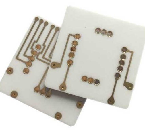
| Assumed uniform heat-flow area | Ceramic resistance | Rise at 8 W |
|---|---|---|
| 3 × 3 mm = 9 mm² | 2.9167 K/W | 23.33 K |
| 6 × 6 mm = 36 mm² | 0.7292 K/W | 5.83 K |
| 12 × 12 mm = 144 mm² | 0.1823 K/W | 1.46 K |
The area assumption can dominate the answer
The familiar ceramic-layer relation R = t/(kA) is useful only when its geometry and boundary conditions are understood. For a small die on a larger ceramic PCB, the die footprint, copper island and board outline are different areas. Selecting one without explanation can change the calculated resistance by an order of magnitude. Start with a clearly labeled one-dimensional estimate and show its sensitivity to area. The thermal-management guide describes the wider assembly; this calculation isolates the ceramic layer so that its assumptions remain visible rather than becoming a misleading junction-temperature claim.
Derive the slab relation and identify its limits
For steady one-dimensional conduction through a uniform slab, heat flow is Q = kAΔT/t. Rearranging gives thermal resistance ΔT/Q = t/(kA). The model assumes constant conductivity, a constant cross-sectional area, and temperatures that can be represented at the two plane boundaries. It does not automatically include the die, attachment layer, top copper, bottom attachment, cooler or contact resistance. It also does not describe how heat spreads sideways between differently sized boundaries. Keep those exclusions next to the result, particularly when the input area is much smaller than the ceramic outline.
Worked example with three explicitly assumed areas
Take a hypothetical ceramic thickness of 0.63 mm and conductivity of 24 W/m·K. A 3 by 3 mm die footprint gives A = 9 mm² and a slab resistance of 2.9167 K/W. Using a 6 by 6 mm area gives 0.7292 K/W, and using a 12 by 12 mm area gives 0.1823 K/W. At an assumed 8 W through the layer, the corresponding rises are 23.33, 5.83 and 1.46 K. These are three different model geometries, not three measured states of the same board. The table is a sensitivity exercise that shows how strongly the answer depends on the selected area.
Do not call the area sweep a rigorous bound
It is tempting to label the footprint calculation the upper bound and the full-board calculation the lower bound. That requires boundary conditions and a physical argument that this simple sweep does not supply. Contact restrictions, nonuniform heat generation, nearby heat sources, finite copper patterns and mounting conditions can invalidate an assumed bound on the complete device temperature. Describe the sweep as sensitivity to a chosen effective area. If a decision changes across the sweep, it is evidence that the area assumption needs a more detailed model or measurement, not permission to select the favorable value.
Use the actual conductor pattern in a spreading assessment
A large board outline does not mean heat can instantly use its full area. Lateral paths depend on the copper pattern, thickness and material, and on what lies below the ceramic. Narrow necks, cutouts and isolated islands can change those paths. Infineon's module-design discussion identifies heat spreading and chip placement as contributors to module thermal behavior, including interaction between adjacent chips. This supports examining the actual layout rather than assigning the outline area to every die. Bring the relevant dimensions from the copper-thickness review into the thermal model.
Check units before comparing materials
Convert thickness to meters and area to square meters when conductivity is in W/m·K. In the example, 0.63 mm becomes 0.00063 m and 9 mm² becomes 0.000009 m². Confusing mm² with m² creates a factor-of-one-million error. Record the conductivity source and its test temperature: Rogers' named ceramic data provide useful reference values, but they are not universal values for every grade and operating temperature. Use the material-data guide to keep the grade and conditions with the number. The arithmetic should be reproducible from the recorded inputs.
Distinguish a ceramic improvement from a system improvement
Changing the assumed conductivity while holding the same thickness and effective area fixed can compare the isolated layer. It does not establish the percentage reduction in the complete thermal path. If attachment and cooling dominate, a large layer improvement can produce a modest device-temperature change. Conversely, a small absolute reduction can still matter near a design limit. Use the AlN thermal-path screening article for the resistance-share calculation. Keep that material-choice question separate from the uncertainty in area; changing both together makes it harder to explain why the result moved.
Decide when a more detailed model is necessary
Escalate beyond the slab estimate when a small hot spot, multiple interacting dies, transient pulses, strongly patterned copper or a localized cold-side contact controls the decision. Define the geometry, power map, temperature-dependent properties and boundary conditions in the model before increasing numerical detail. A fine mesh does not correct a wrong mounting assumption. Compare the model with temperatures or thermal impedance measured at defined locations and power conditions. Record what was calibrated and what remains independent evidence. For an initial check, use the thermal-resistance calculator to reproduce the slab arithmetic and expose input mistakes.
Report a calculation that another engineer can challenge
A useful calculation record contains the purpose of the estimate, the ceramic grade, thickness, conductivity, heat-flow area, power through the modeled layer and excluded resistances. Include a sketch naming the two temperature boundaries and show at least one sensitivity that could change the decision. State whether the result is a preliminary screening value, a calibrated approximation or a validated design result. Do not turn a preliminary estimate into an acceptance limit by removing its assumptions from the final report. The next engineer should be able to identify which physical observation would confirm or overturn the conclusion.
Keep the calculation boundary visible in every result
Draw a line around the ceramic layer and name its upper and lower temperature boundaries. If a report later labels the result junction-to-ambient resistance, the boundary has changed and additional contributions must be included. For a nonuniform temperature field, a single boundary temperature also needs a definition: it might be a specified point, an area average or another quantity used by the model. These definitions are not interchangeable. Keep the heat flow through the boundary consistent with the temperature difference used to calculate resistance. When some heat leaves through leads or another path, total device dissipation is not necessarily the heat passing through the ceramic. The purpose of this sketch is to make such assumptions visible before a convenient number is copied into a system spreadsheet.
Calculate a controlled material comparison
Using the same hypothetical thickness of 0.63 millimeters and area of nine square millimeters, changing the assumed conductivity from twenty-four to one hundred seventy watts per meter kelvin changes the slab result from approximately 2.917 to 0.412 kelvins per watt. The isolated-layer decrease is about 85.9 percent. These inputs are a screening comparison, not a promise for arbitrary alumina and aluminum nitride products. If the rest of a hypothetical thermal path contributes three kelvins per watt, the corresponding total decreases from about 5.917 to 3.412, or approximately 42.3 percent. This calculation holds geometry and every other resistance constant. A real substitution may change interfaces and spreading, so its measured system benefit requires an assembly-level comparison.
Explore thickness and conductivity uncertainty separately
Suppose the nominal screening inputs are subject to an illustrative ten-percent range in conductivity and a five-percent range in thickness. With area fixed, the largest slab resistance relative to nominal is obtained by combining the thicker layer with the lower conductivity: the ratio is 1.05 divided by 0.90, approximately 1.167. The smallest is 0.95 divided by 1.10, approximately 0.864. These are deterministic corner calculations for the assumed ranges, not confidence intervals or manufacturing tolerances. They show why the uncertainty should be tied to each input rather than attached as an unexplained percentage to the final answer. If the effective area is also uncertain, examine it independently; mixing all uncertain assumptions into one favorable case obscures what must be measured.
Avoid double counting spreading in a resistance network
A simplified thermal network may contain a package resistance, a ceramic-layer resistance and an interface resistance. Before adding them, establish the boundaries of each term. A published package value can already include spreading through some internal layers, while a fitted board value may represent several physical layers together. Adding a separately calculated resistance for a layer already represented by another term counts that contribution twice. Conversely, leaving a contact out because it has no convenient data-sheet number can make the network optimistic. Annotate the temperature nodes and heat-flow branches, and distinguish independently measured values from parameters fitted to one experiment. The arithmetic of a series sum is straightforward; deciding whether the physical paths actually form that series chain is the substantive engineering work.
Treat a local cooler contact as part of the geometry
The ceramic outline can be much larger than the area actually coupled to a cooler. A central contact patch, peripheral support or patterned attachment layer changes the path by which heat reaches the cold boundary. A calculation that assumes the entire lower face is isothermal should therefore identify the physical arrangement capable of producing that condition. If the lower copper spreads heat toward a restricted contact, model that spreading rather than assigning the whole board area to a uniform vertical path. When comparing experiments, keep the contact footprint, interface preparation and applied mounting condition consistent. Otherwise, a supposed material improvement can be dominated by a changed cold-side contact that was omitted from the calculation record.
Define what a numerical model adds to the screening estimate
A more detailed model should answer a decision that the slab estimate cannot resolve, such as local peak temperature, interaction between two dies or sensitivity to a copper interruption. Start with a simplified geometry whose result can be checked against an analytical case, then add the necessary detail. Refine the spatial discretization around heat sources and strong gradients while checking whether the quantity of interest changes materially. Convergence of a numerical result is not proof that the material properties or boundary conditions are correct. Keep a list of assumptions that cannot be established by mesh refinement, such as interface conductance and the actual power map. A useful model report explains which uncertainty was reduced by adding detail and which uncertainty remains.
Use transient operation only with a time-dependent model
Steady resistance describes the relationship after the relevant temperature field has stabilized under the assumed conditions. It does not give the peak temperature during every short pulse merely by multiplying instantaneous power by that resistance. A time-dependent model needs thermal storage as well as conduction, and a pulse train may accumulate heat between pulses. Record pulse duration, repetition, duty cycle and the initial condition when analyzing intermittent operation. If a supplier gives transient thermal impedance, confirm its reference boundaries and the applicable mounting condition. Do not combine a transient package curve and an unrelated steady board resistance without explaining the approximation. The slab estimate remains useful as one steady reference point, but it does not establish pulse capability.
Plan a measurement that could disprove the chosen area
To investigate the effective-area assumption, compare temperature measurements at more than one location under controlled power and cooling conditions. A single fitted temperature can often be matched by changing an uncertain contact resistance, so it may not distinguish competing spreading assumptions. Additional spatial measurements or a controlled geometry change can provide more information about the heat path. State the measurement uncertainty and avoid interpreting a difference smaller than that uncertainty as evidence for one material or model. Keep the validation data separate from the observations used to tune uncertain parameters where practicable. The desired outcome is a calculation whose limitations are understood and whose key assumption can be tested, rather than a number that appears precise because many decimal places were retained.
Engineering example
Assumed t = 0.00063 m, k = 24 W/m·K and Q = 8 W. For A = 9 × 10⁻⁶ m², R = 0.00063/(24 × 9 × 10⁻⁶) = 2.9167 K/W. The area sweep changes the model geometry and is not a validated bound on junction temperature.
Before you release the design
- Name both temperature boundaries and excluded layers.
- Show why the chosen heat-flow area is appropriate.
- Convert mm and mm² consistently to SI units.
- Use grade- and temperature-specific conductivity.
- Use a spreading or transient model when the slab assumptions control the decision.
Sources and further technical reading
Manufacturer references support the material and process context. Worked examples and checklists are engineering guidance; they are not test results or supplier guarantees.