
| Hypothetical measurements or model | Result | Scope |
|---|---|---|
| 20,22,25,28,30 micrometers | Mean25; maximum deviation20% | Five sample points only |
| Range divided by mean | 40% | Different metric from half-range/mean |
| 20 mm × 0.5 mm copper strip at20 micrometers | 34.4 milliohms | Assumed constant resistivity |
| Same strip at30 micrometers | 22.93 milliohms | Not a current or thermal rating |
Identify the copper formation route first
Copper thickness uniformity means different things on different ceramic circuit constructions. A bonded copper foil patterned by etching is not the same process as copper built by electroplating over a conductive seed. Some constructions can include both an initial metal layer and subsequent deposition. Identify which operation creates the thickness being specified before discussing plating uniformity. The DPC process guide explains one ceramic metallization route in which deposited layers are relevant. Do not apply an electroplating diagnosis automatically to every DBC or AMB substrate simply because the finished conductor is copper. Start with the actual supplier process and its measurement boundary.
Define the thickness that the drawing controls
State whether the requirement applies to deposited copper only, total copper above the ceramic, a finished conductor after subsequent processing or a specific plated feature. Identify any seed layer and overlying finish separately. A nominal plating target is not necessarily the minimum finished conductive thickness. Also define the location and orientation of the measurement, especially where a feature has sidewalls, a via or a nonrectangular profile. The copper thickness guide provides broader design context. A production requirement becomes measurable when the supplier and customer agree which physical boundary is being measured and which processing steps have already occurred.
Separate panel-scale and feature-scale variation
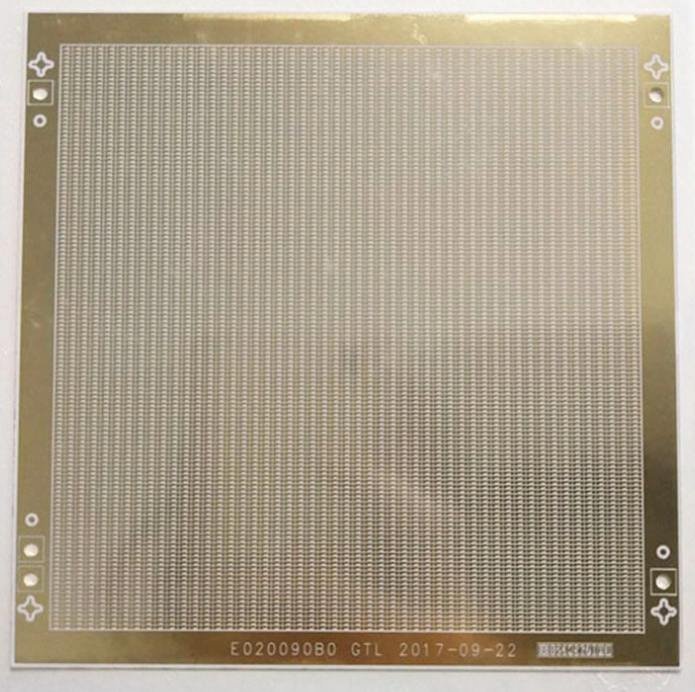
A panel may have a thickness trend from its center to its edges while also showing differences between pads and narrow lines within one circuit. These are different spatial scales. Atotech's panel-plating research explicitly distinguishes within-panel and within-unit distribution in its fan-out packaging studies. Those experiments concern their stated organic and glass panel constructions, not a demonstrated ceramic process window. The distinction is still useful when planning a ceramic measurement map: sample both panel positions and relevant feature types. An average value from several large pads cannot establish the minimum thickness on narrow traces elsewhere in the circuit.
Use uniformity metrics that can be reproduced
Specify the mathematical definition behind a reported uniformity percentage. Consider five invented measurements of twenty, twenty-two, twenty-five, twenty-eight and thirty micrometers. Their arithmetic mean is twenty-five micrometers, and the largest deviation from that mean is twenty percent. The total range divided by the mean is forty percent, while half the range divided by the mean is twenty percent. These are different reporting conventions applied to identical data. Neither percentage is a capability claim for a supplier. Include the individual measurements, sampling locations and formula so that a customer does not mistake one uniformity definition for another.
Keep minimum thickness visible beside the mean
A mean can remain on target while a critical conductor is locally too thin. For a hypothetical uniform copper strip twenty millimeters long and half a millimeter wide, assume a constant resistivity of 1.72 times ten to the minus eight ohm meters. At twenty micrometers thickness, the calculated resistance is 34.4 milliohms; at thirty micrometers it is about 22.93 milliohms. This rectangular, constant-temperature example excludes contacts and other layers. It illustrates why a minimum cross section can matter electrically. Do not use the result as a current rating or temperature prediction; the real conductor profile and thermal boundary still require assessment.
Connect pattern geometry to the process review
Provide the fabricator with the actual panel artwork and identify large pads, isolated features, dense trace regions and exposed metal near the panel boundary. Ask how the qualified plating process handles these differences rather than assuming that one global thickness target makes every feature equivalent. Keep any temporary plating connections or process features distinguishable from the delivered circuit. If the supplier proposes changes to improve distribution, review their effect on the finished electrical layout and separation process. The relevant question is whether the production construction meets its requirements, not whether an unconnected demonstration coupon can achieve a favorable nominal thickness.
Review electrical contact and seed continuity
Electroplating requires an electrical path to the regions being deposited. Identify the intended panel contact arrangement and how current reaches the features during the relevant process stage. A discontinuity or an unexpected resistance in that path can create a local issue that should not be confused with a global bath setting problem. The supplier should review the seed and contact controls appropriate to its process. Do not infer adhesion from electrical continuity alone, or infer uniform deposit thickness because every feature conducts. These are separate observations that may be related during an investigation but require their own evidence and acceptance criteria.
Treat chemistry, equipment and artwork as a combined system
Atotech's research discusses equipment configuration, electrolyte behavior and waveform choices as parts of its panel-plating development. Uyemura's through-hole plating information likewise describes chemistry functions related to deposit control. These sources support treating deposition as a process system; they do not establish a recipe for an unspecified ceramic panel. Ask the selected fabricator to identify the controlled process window and monitoring methods it uses for the proposed construction. Avoid transferring a current density, additive concentration or agitation setting from a different technology. A useful design review documents compatibility and resulting measurements instead of attempting to prescribe a universal plating recipe.
Evaluate process aids with the finished circuit in mind
Shields, auxiliary features or other process aids may be proposed by a plating specialist to improve distribution. Their suitability depends on the equipment, panel arrangement and electrical connection scheme. Clarify whether each feature remains on the shipped part, is removed during processing or exists only in a fixture. If a change affects delivered copper area, check its electrical potential, thermal effect, spacing and assembly clearance. Do not add decorative or floating copper merely to make the artwork look balanced. Require the supplier to demonstrate the intended improvement using the relevant thickness map while preserving the approved circuit functions and manufacturing controls.
Choose measurement methods for the feature geometry
Thickness measurement methods have different access, calibration and sampling limitations. Agree on a method that can resolve the layer and feature of interest, and document how the measurement separates copper from other materials where necessary. A measurement on a broad flat pad may be easier to obtain than one on a narrow or curved feature, but convenience should not determine the entire acceptance plan. Where destructive sections are used, specify their locations and preparation method. Where a nondestructive method is used, confirm its applicability to the stack and thickness range. Preserve calibration and uncertainty information alongside the reported values.
Build a map that can reveal systematic patterns
Select positions that cover the panel center, edges and relevant corners, together with representative feature types in those positions. Label each measurement with its panel coordinate, circuit location, side and feature identity. Keep the map consistent when comparing lots or process adjustments. If the suspected problem is a local minimum beside a particular geometry, add targeted measurements rather than relying only on the standard grid. A color map can help reveal trends, but retain the numerical data and scale. Different color ranges can make two panels appear equally uniform even when their thickness variation differs materially.
Do not assume the two faces behave identically
For double-sided ceramic circuits, identify the thickness requirement and measurement plan on each face. The patterns, contacts and processing exposure may differ, so matching nominal targets does not establish matching local distributions. Compare the features that matter to the assembly rather than averaging both faces into one number. Review the consequences for conductor resistance, attachment height and the broader mechanical stack where applicable. If one face is intended mainly for thermal attachment and the other carries detailed circuitry, the acceptance questions can differ. Preserve that functional distinction in the drawing and inspection report instead of requiring symmetry without a design reason.
Include processing after plating in the final assessment
The deposit can undergo additional steps before the circuit is delivered or assembled. Identify cleaning, seed removal, etching, finishing and separation operations relevant to the construction, and determine at which stage the specified thickness is verified. A satisfactory measurement immediately after deposition does not automatically describe the finished conductor. Likewise, a final thickness result may not reveal whether an earlier process created a defect at an interface. Keep the manufacturing sequence traceable during troubleshooting. Compare measurements from appropriate intermediate and final stages when necessary to distinguish a deposition issue from material removal or damage introduced later.
Investigate outliers before changing the global target
When one location falls outside the requirement, preserve its position, feature type and process history. Check the measurement and specimen preparation, then compare neighboring features and other panels from the same run. Increasing the nominal target everywhere may conceal the local issue while making other regions excessively thick or changing geometry. A controlled investigation should distinguish isolated measurement error, a local feature effect and a systematic panel trend. Select the corrective action with the fabricator and verify its result on a representative configuration. Do not claim process capability from a single improved panel when the original concern involved variation across production runs.
Tie acceptance to the actual circuit functions
Determine which thickness characteristics affect conductor resistance, attachment geometry, bonding surfaces or other relevant functions. State local minimums, permitted ranges or profile requirements only with an engineering basis and an agreed measurement method. A single uniformity percentage may be insufficient if the design requires a specific minimum at a critical feature. Conversely, a tightly constrained global percentage may add cost without addressing the limiting function. Review the proposed criteria with the fabricator before release. The ceramic manufacturing overview can help organize these process-specific questions, while the final requirement belongs on the controlled product documentation.
Release a traceable thickness report with the drawing
A useful release package identifies the copper formation route, controlled layer boundary, finished thickness requirements, sampling map and measurement method. Include the formula used for summary metrics and retain raw measurements for the agreed inspection sample. Record the material, artwork and process revisions represented by the evidence. When panel size, pattern density or contact arrangement changes, review whether the previous qualification remains representative. Copper plating uniformity is demonstrated through a defined distribution of measurements on the actual construction. It should not be inferred from a bright surface, a nominal plating time or a capability number borrowed from another substrate technology.
Engineering example
Dimensions, measurements and resistivity model are illustrative. No supplier process recipe, ceramic plating capability or current rating is implied.
Before you release the design
- Identify plated versus bonded copper and the controlled layer.
- Measure both panel position and feature type.
- Define the uniformity formula and retain raw values.
- Verify measurement applicability to the actual stack.
- Reassess changes to artwork, contact arrangement and panel format.
Sources and further technical reading
Manufacturer references support the material and process context. Worked examples and checklists are engineering guidance; they are not test results or supplier guarantees.