
| Invented case | Result | Boundary |
|---|---|---|
| 90kΩ upper;10kΩ lower | Resistance ratio9;unloaded voltage ratio0.1 | Define which ratio is specified |
| Upper+0.1%;lower−0.1% | Ratio+0.2002% | Worst-direction assumed errors |
| 20/18ppm/K;common50K rise | Ratio change99.91ppm | Linear coefficients |
| Equal20ppm/K;10K/5K rises | Ratio change99.99ppm | Unequal element temperatures |
| 1MΩ load across10kΩ lower | Voltage ratio0.099108 | Ideal loaded divider |
Define the network function before the ceramic drawing
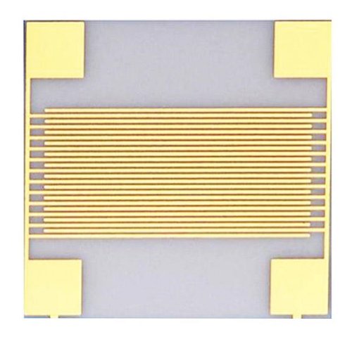
A ceramic resistor network is specified by relationships between resistive elements as well as by the substrate that supports them. A divider, feedback network and independent resistor array can require different electrical definitions even when their outlines are identical. Begin with a labeled schematic, terminal map and list of required measurements. State whether the supplier delivers bare ceramic, patterned conductors, completed resistors or a tested and trimmed network. The single-sided ceramic circuit overview provides one construction context. This article connects the network's functional requirements to the ceramic, layout, process and verification information needed for a useful supplier specification rather than treating substrate material as a complete performance description.
Write the ratio definition explicitly
The word ratio can refer to different mathematical quantities. For an invented divider with a ninety-kilohm upper resistor and a ten-kilohm lower resistor, the upper-to-lower resistance ratio is nine, while the unloaded output-to-input voltage ratio is one tenth. The reciprocal divider factor is ten. These numbers describe the same nominal circuit but are not interchangeable acceptance limits. Ohmcraft's specifying tutorial flags ratio definition as an item that must be clarified. Put the actual equation and terminal identities on the electrical specification. If several ratios matter, name each one separately so trimming, test software and customer verification all evaluate the intended quantity.
Distinguish absolute tolerance from ratio tolerance
Two resistors can each deviate from their nominal value while preserving their required relationship. Conversely, individually acceptable values can produce an unacceptable ratio when their errors oppose each other. As an invented example, let the upper resistor be one tenth of one percent high and the lower resistor one tenth of one percent low. The upper-to-lower ratio is multiplied by 1.001 divided by 0.999, giving an increase of about 0.2002 percent. This is worst-direction arithmetic for those assumed errors, not a production distribution. Specify absolute values and ratio limits independently where the circuit needs both, and identify which requirement governs the final trim and acceptance decision.
Separate absolute TCR from tracking
Vishay's thin-film array application note distinguishes tolerance matching, temperature-coefficient tracking and relative drift as separate network properties. A low absolute temperature coefficient for each resistor is not a complete statement of their relative behavior. Define the required temperature range, reference temperature and ratio being assessed. If a simplified linear model is used during design, label it as an approximation and preserve the sign of each coefficient. Do not combine the most favorable absolute and tracking values from unrelated product families into one assumed custom-network capability. Obtain the performance commitment for the selected resistor technology, substrate and manufacturing route, then verify it under the conditions stated in the specification.
Calculate tracking sensitivity under a common temperature change
For an invented linear example, assume the upper resistor has a coefficient of twenty parts per million per kelvin and the lower resistor has eighteen. Under a common fifty-kelvin increase, their resistance multipliers are 1.001 and 1.0009. The resulting change in the upper-to-lower ratio is about 99.91 parts per million. The usual first-order estimate from the coefficient difference gives one hundred parts per million, close in this small-change example. Neither result includes curvature, self-heating differences or long-term drift. This calculation helps allocate a ratio error budget, but it does not establish that a real network follows constant coefficients throughout the required operating range.
Treat temperature differences as a separate input
Good tracking under a shared temperature change does not by itself describe unequal element temperatures. Consider two invented elements with the same twenty-parts-per-million-per-kelvin coefficient. If one rises ten kelvin from the reference condition and the other rises five, the ratio multiplier is 1.0002 divided by 1.0001, corresponding to about 99.99 parts per million of change. Their coefficients match, but their temperatures do not. This is a sensitivity illustration rather than a prediction for a ceramic network. It shows why the layout and mounting review should identify potential temperature differences instead of relying only on a catalog tracking value measured under a defined common environment.
Map the actual power distribution
For the ninety-kilohm and ten-kilohm divider introduced earlier, an invented ten-volt input produces one hundred microamperes in the unloaded series path. The upper resistor dissipates nine tenths of a milliwatt and the lower one tenth of a milliwatt. The dissipation is unequal even though both elements carry the same current. Use the circuit's real operating conditions to create a power map for the network, including any relevant duty cycle or neighboring heat source. Do not infer element temperature directly from these powers without a thermal model or measurement. The calculation identifies a condition to investigate and helps the supplier understand why element placement or geometry may matter to the required ratio stability.
Specify the substrate as part of the resistor process
The ceramic request should identify the grade, thickness, surface condition and dimensional requirements needed by the chosen resistor and conductor process. Agree which properties are controlled by the substrate manufacturer and which are established during network fabrication. A material-family label alone does not establish compatibility with every resistive composition or deposition method. The thick-film and thin-film comparison helps distinguish manufacturing routes, but it is not a substitute for process-specific evidence. When comparing quotations, check that both suppliers are offering the same delivered state and functional verification rather than comparing a bare tile with a completed precision network under the same product name.
Connect placement to the installed thermal environment
Describe the mounting arrangement and nearby sources of heating or cooling that can influence the network. Identify whether one end is close to a warm component, a large terminal or a mechanically constrained contact region. Ask how the proposed layout will be evaluated under the relevant installed conditions. A common ceramic can support thermal coupling, but the degree of temperature uniformity in a custom assembly should be established rather than assumed from another product's example. The thermal management guide provides a broader framework for defining boundaries. Keep the temperature observations and operating conditions linked to the network revision so ratio changes can be interpreted in context.
Reserve the features needed for trimming and measurement
If the network requires trimming, define the final electrical targets and discuss the necessary physical access with the fabricator. The layout must accommodate the qualified trim method, measurement contacts and any protective processing that follows it. Do not place a critical terminal or neighboring feature in a region needed for the intended operation without agreement. Record whether acceptance occurs immediately after trimming or after subsequent processing and stabilization. A network that meets its ratio at one intermediate stage may require another check in the delivered state. This distinction belongs in the manufacturing and test plan, not merely in an informal conversation about how accurately a resistor can be adjusted.
Define the role of conductor and terminal resistance
The measured network includes the connections present between the chosen test terminals. For low-value elements or demanding ratios, conductor and contact contributions can affect the result. Identify where voltage is sensed and current is applied, and decide whether the required value includes the external terminal connection. If separate sense connections are used, document their relationship to the resistor elements and preserve that arrangement in acceptance testing. Avoid assigning an ideal resistor value in the schematic while leaving the physical measurement endpoints undefined. The substrate layout and test fixture should implement the same electrical boundary that the specification uses, allowing supplier and customer measurements to be compared meaningfully.
Include loading in the divider requirement
A divider ratio measured without a load may differ from the ratio in the operating circuit. In the invented ninety-kilohm and ten-kilohm network, placing a one-megohm load across the lower resistor changes its effective value to approximately 9.901 kilohms. The resulting output-to-input ratio is about 0.099108 rather than 0.100000, a relative reduction of about 0.892 percent. This ideal circuit calculation excludes other input effects. It demonstrates why the required ratio must state the measurement load or input impedance. A substrate or trim change cannot correct an undefined system boundary, and a supplier's unloaded acceptance result should not be compared directly with a loaded circuit measurement.
Keep voltage, power and environmental requirements distinct
A network specification should identify the relevant electrical and environmental conditions rather than assuming that meeting the resistance ratio establishes all other requirements. Element voltage, total power, insulation between nodes and any required transient behavior address different questions. Define the conditions and verification methods appropriate to the intended application with the responsible circuit and product engineers. If environmental exposure or subsequent assembly processing is expected, state the delivered configuration and the post-exposure properties that matter. This allows the manufacturer to assess the complete request and prevents a high-precision ratio claim from being mistaken for a qualification of every voltage, power or service condition the network might encounter.
Separate initial accuracy from stability over time
A trim or initial test establishes performance at the stated acceptance condition. It does not alone establish how the relationship between elements changes after extended operation or environmental exposure. Define any required stability measure using a named ratio, baseline measurement and test condition. Keep absolute resistance drift and ratio drift separate when both matter. Vishay's array discussion identifies relative drift as a distinct consideration; its product example should not be generalized into a lifetime guarantee for another construction. Request evidence appropriate to the custom network and preserve the test duration and conditions rather than reducing the result to a single stability adjective without a measurable definition.
Use a measurement plan that can resolve the requirement
Choose measurement conditions and equipment that can distinguish the required acceptance limit from measurement uncertainty and setup effects. Record fixture identity, connection method, settling approach, measurement power and temperature information relevant to the result. Avoid changing the load or self-heating condition between the supplier's test and incoming verification without accounting for the difference. If a reported ratio changes after the network is installed, compare the measurement boundaries and thermal conditions before concluding that the ceramic or resistive film has changed. A reproducible test plan makes disagreement actionable because each team can see what was actually measured and which assumption needs to be checked.
Release the network with linked electrical and substrate records
The final specification should connect the schematic and terminal map to absolute values, ratio equations, tracking requirements, power distribution, substrate details and the delivered test state. Include the evidence supporting any stability or environmental claim and identify the operating boundaries not covered by that evidence. Keep revisions synchronized when the ceramic, resistor process, terminal layout or protective layer changes. A ceramic resistor network is useful because its elements can be engineered and verified as a connected system. The procurement record should preserve that system definition so a future supplier or design change can be assessed against the same functional relationships rather than only against an outline and a list of nominal resistances.
Engineering example
All numerical networks are invented sensitivity examples,not specifications or ratings for a supplier product.
Before you release the design
- State ratio equations and terminal identities.
- Separate absolute tolerance,tracking and drift.
- Map power and thermal gradients.
- Control trim and measurement access.
- Specify loaded and delivered test conditions.
Sources and further technical reading
Manufacturer references support the material and process context. Worked examples and checklists are engineering guidance; they are not test results or supplier guarantees.