
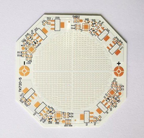
Start with the device heat path
Use dissipated heat rather than input electrical power when the optical output is significant. Include die attach or package thermal resistance and the interface to the heat sink. The LED footprint and local heat-flow area matter more than total board area in an initial hot-spot assessment.
Coordinate optical and electrical details
Reflective layers, solder mask, pad finishes and nearby metal can affect optical performance. Define color, reflectance or stability requirements only when they are functional. Confirm that assembly heating and cleaning do not compromise the chosen optical surface.
Choose ceramic and process by the construction
Alumina may provide an economical baseline; AlN can help when the ceramic thermal path is limiting. DPC, printed films and other qualified constructions support different pad geometries. Validate the completed assembly at its intended drive conditions and cooling setup.
Engineering example
For a dense LED array, increasing the board outline may not meaningfully lower the hottest die temperature if the die attach and local substrate path dominate. Compare changes with a spatial thermal model.
Before you release the design
- State dissipated heat and LED footprint.
- Specify finish and optical surface requirements.
- Measure temperatures in the actual cooling arrangement.
Sources and further technical reading
Manufacturer references support the material and process context. Worked examples and checklists are engineering guidance; they are not test results or supplier guarantees.