
| Ideal geometry | Conducting area | Electrical resistance | Axial thermal resistance |
|---|---|---|---|
| Solid 0.30 mm cylinder | 0.07069 mm² | 0.178 mΩ | 25.5 K/W |
| 0.30 mm outside / 0.25 mm inside wall | 0.02160 mm² | 0.583 mΩ | 83.3 K/W |
A filled feature needs a cross-section and a material identity
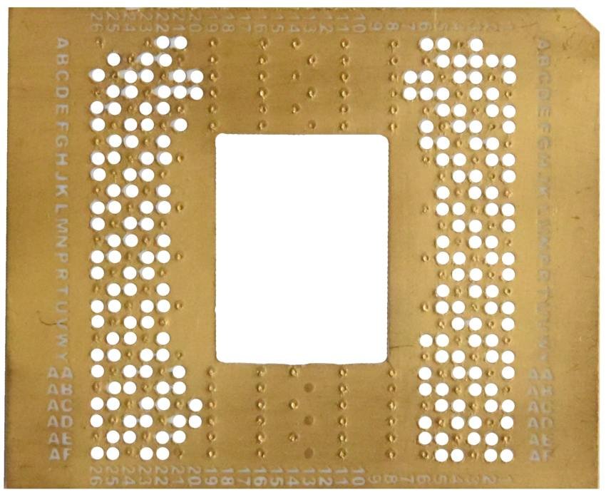
The phrase copper-filled ceramic PCB can describe very different structures. It might refer to a solid copper connection through a fired ceramic, metal deposited on a hole wall, a conductive filling material or copper plated over an underlying metallization. None of these descriptions can be established from a top-view photograph alone. Begin with a cross-section naming the ceramic, the fill, the surface conductors and any intermediate layers. State whether the feature carries current, conducts heat, connects a ground plane or serves several functions. The ceramic process overview provides context for the manufacturing routes. This article focuses on the questions needed to compare filled features without assuming that every conductive hole behaves like a cylinder of bulk copper.
Separate co-fired interconnects from post-fired metallization
Kyocera describes multilayer ceramic wiring in which vias in ceramic sheets are filled with conductive paste before the layers are laminated and co-fired. That description establishes a manufacturing sequence; it does not identify every such via as pure copper. A post-fired ceramic with a drilled or otherwise formed opening and subsequent metallization is a different construction. Ask which sequence applies and which material actually forms the connection. Shrinkage control, registration and achievable geometry depend on the route, so dimensions from one family should not become rules for another. Keep the multilayer ceramic guide linked to the layer definition rather than using multilayer as a catch-all term for any board with metal on both faces.
Use manufacturer examples as evidence of a specific construction
Applied Thin-Film Products describes solid gold or copper filled vias and provides a particular copper-via example with its own carrier and boundary conditions. Remtec separately describes plugged and plated via options in thick-film ceramic structures. These sources show that several engineered interconnect options exist; they do not establish that every supplier offers the same fill, dimensions or qualification. Request a construction drawing and a specification for the proposed product. If a supplier uses a trade name, ask what physical layers and interfaces that name represents in the quoted part. A capability demonstrated in one package is useful starting evidence, but it is not a guarantee for a different ceramic thickness, hole shape or assembly process.
Identify the electrical nodes on both sides of the ceramic
A continuous metal connection through an insulating ceramic changes the electrical topology. If a feature joins the top conductor to a backside cooling surface, those regions are connected unless another defined insulating interface separates them. Do not describe a thermal via as electrically harmless simply because heat transfer is its intended purpose. Mark the net assignment and the relationship to nearby metal, mounting hardware and the cooler. A feature can improve a conduction path while defeating an intended isolation arrangement. Review the creepage and clearance guide with the actual electrical design and applicable requirements. This article does not assign an insulation distance or authorize a connection across a barrier that the system requires to remain isolated.
Worked geometry comparison: solid fill and a plated wall
Consider an invented circular opening with an outside diameter of 0.30 millimeters. A completely solid cylindrical fill has a cross-sectional area of pi times diameter squared divided by four, approximately 0.07069 square millimeters. Now suppose only a uniform wall thickness of 0.025 millimeters conducts, leaving an inside diameter of 0.25 millimeters. The conducting annular area is pi times the difference between the squared diameters divided by four, approximately 0.02160 square millimeters. The solid area is about 3.27 times larger. These ideal shapes exclude pores, surface layers and dimensional variation. They demonstrate why outside diameter alone is insufficient for comparing a filled hole with a plated hole.
Estimate electrical resistance with an explicitly assumed resistivity
For a uniform conductor, the simple relation is resistance equals resistivity times length divided by cross-sectional area. Using an invented length of 0.63 millimeters and an assumed resistivity of two times ten to the minus eight ohm meters, the solid geometry gives approximately 0.178 milliohms. The plated-wall geometry gives approximately 0.583 milliohms. These values are illustrative, not specified properties of a deposited metal or a conductive paste. They exclude the interfaces and surface routing that connect the feature to the rest of the circuit. Actual resistivity depends on the material and condition, and resistance changes with temperature. Use the calculation to identify which construction details are missing before treating a supplier's nominal via diameter as an electrical specification.
Do not convert low resistance directly into an allowable current
At an assumed current of ten amperes, the preceding ideal resistances would produce about 0.0178 watts and 0.0583 watts of resistive heating respectively. That arithmetic does not establish an allowable current for either feature. The temperature rise also depends on heat removal, neighboring losses, material properties and the connections at both ends. A manufacturer's current demonstration belongs to its specimen, temperature criterion and mounting condition. In particular, an isolated via attached to a substantial metal carrier cannot be assumed equivalent to a dense array under a small component. Define the intended current waveform and permitted thermal condition, then validate the complete path. The trace-resistance tool can check simple conductor arithmetic but does not qualify a ceramic via.
Calculate a thermal path without mistaking it for the whole board
For the same ideal cylinders, using a deliberately assumed conductivity of three hundred fifty watts per meter kelvin gives a through-feature resistance of length divided by conductivity and area. The solid cylinder is approximately 25.5 kelvins per watt, while the plated wall is approximately 83.3 kelvins per watt. These numbers describe only axial conduction in the ideal metal geometry. The surrounding ceramic also conducts heat, and the surface layers distribute heat into and out of the feature. Consequently, these values should not be reported as the board's total thermal resistance. The comparison shows the influence of conducting area while keeping the other assumptions fixed; a useful board model must add the actual parallel and spreading paths.
Use parallel-via arithmetic only within its assumptions
If ten identical ideal solid vias share the same temperatures at their ends and carry heat independently, their combined axial resistance is one tenth of a single via's value. That follows from adding parallel conductances. Real arrays can depart from this model because the top metal cannot distribute heat uniformly, the bottom contact is restricted or neighboring vias compete for spreading area. Electrical current sharing also depends on the routes feeding the array and contact resistance at the ends. Preserve the ideal calculation as a reference rather than multiplying a single-via rating by the number of holes. A dense pattern can improve some paths while reducing ceramic ligament widths or complicating manufacturing, so array geometry needs its own review.
Specify the end condition and local surface topography
A filled hole may terminate flush with the surface, below it or above it, depending on the process and finishing operations. That condition can matter when a component or attachment layer spans the feature. Define the relevant surface and the allowed geometry using a method the supplier can inspect. Do not assume that a visually closed opening is internally solid or that a conductive fill is automatically planar enough for an attachment operation. Include the relationship between the fill and any overlying metallization. If the end is capped, identify the cap material and connection. A cross-section and surface profile answer different questions, and both may be needed when the feature lies beneath a critical die-attach area.
Treat voiding and cracks as measured features, not labels
Ask how the supplier detects incomplete fill, discontinuities and separation at the ceramic or conductor interfaces. Define which defect descriptors affect acceptance and which inspection method can establish them. A two-dimensional image does not necessarily reveal the depth or connectivity of every internal feature. A destructive section shows the plane that was cut, not the entire volume automatically. Use representative sections during process qualification and suitable production inspection where justified by the requirement. Avoid importing a solder-joint void percentage as a universal fill criterion for a different material system. The relevant question is whether the observed condition threatens the required electrical, thermal, mechanical or sealing function under the specified operating conditions.
Keep hermeticity separate from electrical continuity
A low-resistance connection is not proof that a feature prevents gas or moisture leakage. Conversely, a sealing result does not establish the current capacity or thermal resistance of the conductor. When hermetic behavior is required, state the tested boundary, method and acceptance criterion in the package specification and identify whether the via or the complete enclosure is being evaluated. Manufacturer descriptions of hermetic plugged vias apply to their qualified constructions and should not be generalized to every filled hole. Retain the test configuration and any post-assembly exposure that could affect the seal. Do not assign a leak-rate requirement merely because another package catalog uses it; connect the requirement to the actual product and verification method.
Evaluate expansion and assembly exposure at the interfaces
Metal and ceramic respond differently to temperature, and the stress developed around a filled feature depends on geometry, constraints and material behavior. The existence of an expansion difference alone does not predict a crack or a service life. Document the relevant assembly temperature history, attachment steps and service exposures, then select a qualification program that addresses the actual construction. Examine the feature interfaces and functional results before and after that program. A change in hole diameter, fill material or ceramic thickness can alter the mechanical situation even when initial resistance remains similar. Keep those changes under review instead of treating the via as an interchangeable library element with only two electrical terminals.
Make a supplier comparison table that exposes missing data
For each candidate, record the ceramic grade and thickness, opening geometry, actual conducting material, fill or wall dimensions, surface termination and connection to each conductor layer. Add measured resistance conditions, thermal evidence where required, inspection coverage and any sealing claim with its test basis. Separate guaranteed acceptance values from representative demonstrations. Mark unknown fields as questions rather than estimating them from unrelated marketing images. The DFM checklist can organize this discussion. A candidate with a slightly larger nominal feature may be easier to validate than one with an impressive dimension but an undefined fill or inspection method. Select on the complete functional evidence rather than the smallest quoted hole.
Release the feature as part of a controlled stack-up
The final drawing should include a section, net assignment, dimensional definitions and the acceptance evidence needed for the feature's intended functions. Link the via to the stack-up specification so that a later ceramic, finish or attachment change triggers the appropriate review. Preserve the calculations as explicitly idealized screening results and replace assumed inputs with supplier-specific data where those inputs control the design. Do not describe a research concept or an optional process capability as a qualified production feature before the actual part has been evaluated. A well-defined copper-filled structure is valuable because its interfaces and limits are understood, not simply because the word copper appears in its name.
Engineering example
Invented model: length0.63mm, resistivity2×10⁻⁸Ω·m and conductivity350W/m·K. Geometry excludes interfaces, porosity, spreading and the parallel ceramic path. None of these values is an allowable current or a guaranteed product property.
Before you release the design
- Identify the actual fill and process sequence.
- Draw all interfaces and both electrical nodes.
- Use conducting area rather than outside diameter alone.
- Keep current, thermal and hermetic qualification separate.
- Validate the complete feature and array under the actual assembly conditions.
Sources and further technical reading
Manufacturer references support the material and process context. Worked examples and checklists are engineering guidance; they are not test results or supplier guarantees.