
| Illustrative ceramic layer | k at 20°C | Assumed thickness | R at 100 mm² | Drop at assumed 100 W |
|---|---|---|---|---|
| curamik Performance Si₃N₄ | 90 W/m·K | 0.32 mm | 0.0356 K/W | 3.56 K |
| curamik Thermal AlN | 170 W/m·K | 0.63 mm | 0.0371 K/W | 3.71 K |
| curamik Power Al₂O₃ | 24 W/m·K | 0.63 mm | 0.2625 K/W | 26.25 K |
Start with the module boundary, not an 800 V material label
An 800 V traction inverter does not have one universally correct ceramic PCB stack-up. Choose a copper-clad ceramic construction against the actual voltage stresses, loss map, cooling arrangement and lifetime target. In this context, ceramic PCB means the power substrate carrying the switches, not necessarily the separate gate-driver board. The design deliverable is a controlled assembly drawing plus verification requirements. Our EV inverter overview describes the application; this guide turns those requirements into a comparison of candidate stacks.
Write the complete stack before comparing materials
For a conventional single-sided heat path, list the die, die attachment, patterned top copper, metal-to-ceramic joining layers, ceramic, bottom copper, substrate attachment or thermal interface, and cooler. Include a baseplate if the architecture uses one. Do not accidentally count a baseplate-to-cooler interface in a directly cooled design, or omit it from a conventional module. Record nominal thickness, tolerance, contact area and responsible supplier for every layer. The stack-up specification guide provides the general drawing framework. Treat metallization, joining layers and surface finish as separate entries wherever they affect assembly or inspection.
Keep grade and process tied to each candidate
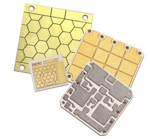
Silicon nitride AMB is worth evaluating when mechanical robustness is central; AlN is worth evaluating when the ceramic layer is a significant thermal bottleneck. Alumina DBC remains a useful baseline if its thermal and reliability results satisfy the requirements. These are candidates, not a ranking of approved automotive products. Rogers lists 90 W/m·K at 20°C for curamik Performance silicon nitride and 170 W/m·K for curamik Thermal AlN in its technical sheet. Its separate Performance Plus silicon nitride product lists 110 W/m·K at 20°C. Specify the named grade: replacing 90 with 110 in a model without changing the purchase specification creates an unsupported improvement. See the silicon nitride material guide for the broader selection context.
Screen thickness using an explicit heat-flow area
Use R = t/(kA) for an initial through-thickness ceramic calculation, with thickness t in meters, conductivity k in W/m·K and area A in square meters. The table below uses an assumed 100 mm² area and room-temperature reference conductivity. It compares ceramic layers only. A smaller die footprint, lateral spreading in copper, neighboring dies and temperature-dependent conductivity change the real heat flow. Use the thermal-resistance calculator to vary assumptions, then move to a model with the actual geometry. Do not interpret this screening result as junction-to-coolant resistance or proof that any listed thickness meets insulation requirements.
Treat copper as part of the mechanical and thermal design
Increasing copper thickness can improve lateral heat spreading and reduce conductor resistance, but it also changes the forces imposed on a brittle ceramic during temperature excursions. Review top and bottom patterns together, including large copper islands, narrow necks, edge setbacks and local asymmetry. A nominally symmetric thickness specification does not guarantee symmetric copper coverage. Ask the fabricator to review the finished artwork, etch profile and available corner geometry. Keep the selected AMB manufacturing process attached to the drawing revision; changing the joining process or ceramic grade can invalidate the evidence supporting the original stack.
Separate three insulation questions
Infineon's automotive insulation-coordination note distinguishes clearance through air, creepage along surfaces and solid insulation. It also distinguishes working, recurring peak and transient voltages. An 800 V nominal bus label therefore cannot determine the ceramic thickness or all spacing requirements. Document maximum operating voltage and relevant transients, insulation function, altitude, environment and the actual insulating surfaces. Review the substrate edges, encapsulant and terminals as part of the assembled module. The supplier's example dimensions and test conditions belong to its particular module; they are not universal drawing values. Use the creepage and clearance guide to organize the review, and have the applicable product requirements and test plan established for the final assembly.
Use interface sensitivity to decide where to spend effort
Suppose the rest of an illustrative thermal path contributes 0.30 K/W. Adding a 0.32 mm, 90 W/m·K ceramic over the assumed area gives about 0.336 K/W; replacing it with a 0.63 mm, 170 W/m·K ceramic gives about 0.337 K/W. The difference is negligible in this simplified model despite the higher conductivity of AlN. If a contact interface instead adds 0.10 K/W, improving that interface has far more potential than this material substitution. These assumed resistances are not measured module data. Use them to structure a sensitivity study, then replace them with geometry-specific models or measurements under controlled mounting and cooling conditions.
Qualify the failure mode, then freeze the construction
A thermal result at one operating point does not establish cycling life. Review die attachment, substrate attachment, interconnects, ceramic cracking and cooling contact separately. Infineon's power- and temperature-cycling application note illustrates why different interfaces and test conditions matter; a cycle count cannot be transferred blindly between constructions. For each candidate, request the actual temperature excursion, dwell or pulse duration, monitored parameter and failure criterion behind the supplier's evidence. Compare those conditions with the intended mission profile. Before release, define which changes trigger review: ceramic grade, copper pattern, joining process, attach material, finish, mounting method or encapsulation.
Make the supplier comparison reproducible
Send every supplier the same drawing revision, loss assumptions, cooling boundary and electrical acceptance requirements. Request proposed deviations explicitly rather than accepting an unlabeled equivalent material. Keep a decision log with three columns: requirement, evidence and remaining uncertainty. A candidate that is a little better in the first-order thermal calculation may still require more work to establish mechanical or electrical suitability. The defensible choice is the construction with adequate performance and evidence for the actual assembly, supported by production controls that preserve those conditions.
Engineering example
Calculation check: 0.00032 m / (90 W/m·K × 0.0001 m²) = 0.03556 K/W. At an assumed 100 W passing uniformly through that area, the ceramic-only temperature difference is 3.56 K. This excludes all other layers and multidimensional spreading. Table thicknesses are screening choices; no entry represents a qualified 800 V module or a manufacturing offer.
Before you release the design
- Identify the ceramic grade, joining route, copper pattern and every thermal interface on a controlled drawing.
- Replace nominal bus voltage with the project's complete insulation and voltage-stress requirements.
- Compare thermal candidates at explicit areas, thicknesses and cooling boundaries; verify assumptions with the actual assembly.
- Record cycling conditions and failure criteria, not only a supplier's headline cycle count.
- Agree inspection, electrical acceptance and material/process change controls before releasing production.
Sources and further technical reading
Manufacturer references support the material and process context. Worked examples and checklists are engineering guidance; they are not test results or supplier guarantees.
- Rogers — curamik ceramic substrates technical data sheet (grade conductivity and available constructions)
- Rogers — curamik Performance Plus (separate 110 W/m·K silicon nitride grade)
- Infineon — Insulation Coordination in Automotive Power Module, IEC60664-1:2020 (application example, not a universal stack specification)
- Infineon — AN2019-05 PC and TC Diagrams (cycling conditions and interface reliability)