
| Hypothetical screening item | Value | Boundary |
|---|---|---|
| Emitter electrical input | 8 × 6 V × 0.5 A = 24 W | Eight LEDs |
| Other board loss | 1 W | On-board components |
| Conservative assumed board heat | 25 W | All emitter input assigned to heat |
| Shared-path rise | 25 W × 1.4 K/W = 35 K | Board reference to ambient |
| Conditional shared-path target | (70 − 30) / 25 = 1.6 K/W | Invented board temperature budget |
Start with the selected emitter and the complete heat path
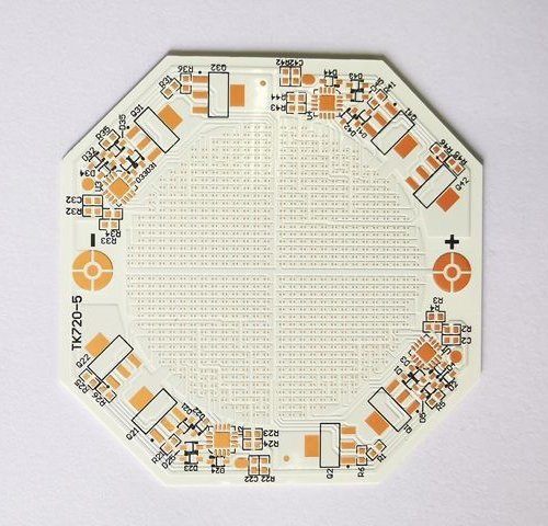
A ceramic PCB can provide electrical isolation and a useful conduction path in a UV LED module, but the material name does not establish the emitter temperature. Begin with the exact LED package, its recommended attachment geometry and the cooling arrangement that will exist in the finished product. A packaged emitter already contains internal thermal interfaces, and the board adds further spreading, attachment and contact contributions. Treat these as an assembly rather than comparing substrate conductivity alone. The ceramic LED board guide describes the carrier options. This article addresses how to create a thermal budget and verify it for a UV module; it does not establish a germicidal dose, curing performance or a permissible human exposure.
Check which power belongs in the supplier's equation
The power convention used to define a thermal resistance matters. A physically defined conduction resistance may be paired with heat dissipated in the device, while a manufacturer may specify an effective thermal parameter and calculation using electrical input. Nichia's SMD UV LED note explicitly defines the power in its junction-temperature equation as forward current multiplied by forward voltage. Use that definition with the corresponding parameter. Do not subtract optical power from that input unless the selected parameter and method require it. Otherwise, a correction intended to improve accuracy can make the temperature estimate inconsistent. Keep the supplier's parameter name, reference point and power definition together in the calculation record rather than copying only a resistance value into a generic thermal spreadsheet.
Separate the energy balance from the temperature-estimation convention
For an energy balance around an emitter, electrical input that leaves as emitted optical radiation is not heat retained at that emitter. However, radiation absorbed elsewhere in the module can become heat at a different location. Define the physical boundary when allocating these loads. A reflective optical component, absorbing enclosure or nearby target is not automatically part of the ceramic conduction path. Record which losses belong to the board and which belong elsewhere in the system. This physical accounting is compatible with following a manufacturer's electrical-input temperature method, provided the two calculations are not mixed without explanation. One calculation allocates energy; the other estimates a temperature using a parameter with a specific definition and test boundary.
Worked example: a conservative preliminary cooling load
Consider an invented eight-emitter module in which each LED operates at six volts and half an ampere. Total electrical input to the emitters is twenty-four watts. For an initial conservative board-load estimate, assume all of that input becomes heat and add one watt of other loss on the board. The resulting assumed cooling load is twenty-five watts. If a hypothetical shared board-to-ambient path is 1.4 kelvins per watt, its calculated rise is thirty-five kelvins at the defined board reference point. This is not an individual junction temperature. Package and local spreading contributions remain to be evaluated, and the assumed shared resistance must be established for the actual mounting and cooling arrangement.
Translate a temperature budget into a conditional cooling target
Suppose, only for a screening exercise, the design owner assigns a board reference-temperature target of seventy degrees Celsius at an ambient temperature of thirty degrees. With the twenty-five-watt assumed load, the available rise is forty kelvins, so the corresponding shared-path target is at most 1.6 kelvins per watt. The earlier hypothetical 1.4 value would leave five kelvins of board-reference margin under those assumptions. Neither the seventy-degree target nor this margin is a component recommendation. The allowable board reference temperature must be derived from the selected emitter's junction limit, thermal method and design margin. Include uncertainty in load, ambient conditions and interfaces before describing a nominal calculation as a qualified design.
Do not treat UV-A and UV-C packages as interchangeable
Select the package documentation for the actual wavelength and device revision. Similar external dimensions do not establish identical electrical input, optical conversion, thermal resistance or measurement location. Nichia's thermal note evaluates named UV-A and UV-C devices separately, which is a useful reminder to retain component identity through the analysis. Do not transfer its plotted temperatures to a different emitter or heat sink. For a multiwavelength module, create separate entries for each device type and state which combinations operate together. Procurement substitutions should trigger a review of the thermal budget as well as the optical and electrical requirements. A shared ceramic footprint can simplify assembly without making every compatible-looking package thermally equivalent.
Model local and shared temperature rises separately
An array has a common cooling path and local paths around individual sources. In a simplified network, one term may describe the temperature rise of a board reference relative to ambient, while another describes the selected device relative to that reference. These terms can be added only when their boundaries and power definitions are consistent. The thermal-management guide helps organize the layer sequence. Do not assign the full array power to every local package resistance, or assign one emitter's power to the shared cooler path. Those errors can produce very different answers while leaving the spreadsheet dimensionally plausible. Draw the network and identify the heat associated with every branch before substituting numerical values.
Consider thermal interaction between neighboring emitters
A local temperature can depend on neighboring heat sources as well as the device located above it. Luminus demonstrates this coupling with temperature matrices for a particular multichip package; those coefficients belong to that package and test construction, not to an arbitrary UV board. For a ceramic array, use the actual emitter spacing, conductor pattern and cooling boundary when investigating interaction. Compare a single active emitter with the intended operating group if the control system changes which emitters are energized. The same total input distributed over different positions can produce a different hottest location. A useful simulation or experiment should therefore preserve the spatial power pattern instead of replacing every operating mode with one average heat source.
Choose ceramic thickness and grade after identifying the bottleneck
For an initial isolated-layer estimate, resistance scales with thickness divided by conductivity and heat-flow area. That relation can compare candidate assumptions, but it does not establish how widely heat spreads from a small LED package. A higher-conductivity ceramic may reduce one contribution while attachment or the cooler interface continues to dominate. Use the ceramic thermal-resistance tool to check units and sensitivity, and keep the assumed area explicit. Do not select the entire board outline as the heat-flow area simply because that produces a low number. If the material decision changes when the area assumption changes, obtain a spreading assessment or measurement before choosing the grade solely on the screening result.
Specify the cold-side contact as a controlled interface
Document the area and condition of the surface that couples the ceramic assembly to the heat sink. Identify the attachment or interface material, the intended bond-line control and the approved mounting procedure. A small contact patch beneath a large board can restrict the available path even when the ceramic itself conducts well. Keep fixture conditions consistent between prototypes so that a material comparison is not actually a comparison of mounting quality. Where the assembly uses a compliant interface, establish its behavior under the intended installation conditions rather than assuming that a catalog conductivity defines the complete contact resistance. The stack-up guide provides a place to record these interfaces with the substrate and metallization.
Account for pulsed drive without relying on average power alone
UV systems may use continuous drive, intermittent operation or modulated pulses. Record the actual waveform, repetition rate, duty cycle and maximum on-state current. Average input is useful for a long-term energy balance, but it does not alone establish the transient junction-temperature peak. The relevant response includes thermal storage and the time between pulses. Follow any transient method provided for the selected component and the applicable test boundary. If a transient model is used, state the initial temperature and whether repeated pulses reach a periodic condition. Do not infer pulse capability from the ceramic material's nominal temperature resistance. Package electrical limits and attachment behavior remain separate constraints that the board material cannot override.
Design a junction-temperature verification method before testing
Choose a measurement approach supported for the emitter and identify its reference point on the assembled board. If a temperature is measured near a solder pad, preserve the location and sensor installation method across samples. A convenient point on the cooler is not automatically the manufacturer's specified reference. Record the actual current and voltage while the thermal measurement is taken, because changing operating conditions can invalidate a comparison. Where optical temperature measurement is used, evaluate the surface and instrument setup instead of assuming every visible surface reports the same temperature accurately. Save the raw readings and the calculation connecting them to the reported junction estimate. A temperature number without that connection is difficult to audit.
Choose operating cases that expose the likely hot region
Test the configuration expected to create the highest relevant temperature under the intended system conditions. This can involve ambient temperature, restricted airflow, a particular emitter grouping or other nearby losses. Select the cases from the product's operating requirements rather than adding arbitrary extremes. Include the actual enclosure and cooling hardware when they affect the boundary. If a laboratory fixture provides better cooling than the product, identify that limitation explicitly. Define the stabilization criterion and record how long the system was observed. A short measurement that ends before the shared structure warms up can miss the operating temperature even if the emitter's immediate surroundings appear stable. Keep the test purpose and acceptance criterion in the same record.
Connect assembly inspection to the thermal decision
The attachment between the emitter and its carrier can influence the local path. Agree the assembly method and inspection criteria using the component and process requirements, rather than applying a universal void percentage to every package. A projected defect fraction alone may not describe its location relative to the heat source. Keep inspection results associated with the specimens used in thermal testing so that an unusual temperature can be investigated against actual assembly evidence. This does not mean every variation in an image predicts a failure; it means that thermal and assembly records should be traceable to the same physical unit. Include any rework history because it may change the assembly conditions being compared.
Release the thermal specification with clear ownership
The final release should identify the approved emitters, drive conditions, ceramic construction, attachment interfaces, cooling boundary, measurement method and acceptance temperatures. Assign responsibility for bare-board dimensions, populated-module inspection and complete-system verification. The RFQ brief builder can help organize the supplier handoff, but the controlled drawings and test specification establish the requirements. Retain the assumptions used for early screening separately from the evidence supporting release. If a later design changes emitter pitch, package, interface material or heat sink, revisit the affected model and test cases. This makes the ceramic selection part of an auditable thermal design instead of a stand-alone claim that a particular material automatically solves UV LED cooling.
Engineering example
The numerical example is invented and is not a UV LED operating recommendation. It uses a conservative energy budget for shared cooling and does not replace the selected manufacturer's junction-temperature calculation or power convention.
Before you release the design
- Keep the thermal parameter and its specified power convention together.
- Identify local and shared temperature boundaries.
- Retain actual emitter identity, spatial loading and drive waveform.
- Specify the cold-side contact and measurement fixture.
- Verify the completed module before accepting a material-only temperature claim.
Sources and further technical reading
Manufacturer references support the material and process context. Worked examples and checklists are engineering guidance; they are not test results or supplier guarantees.