
| Invented screening calculation | Result | Limitation |
|---|---|---|
| 11,000 W × (1/0.97 − 1) | 340.2 W | Total loss within the efficiency boundary |
| (120°C − 65°C) / 20 W | 2.75 K/W | Single-source junction-to-coolant budget |
| 2.75 − 0.80 K/W | 1.95 K/W | Remaining budget only if boundaries are compatible |
Define the power stage before selecting its carrier
An onboard charger contains several functions, and they do not all impose the same requirement on a ceramic substrate. Identify the devices and circuit section that the carrier supports, its electrical potentials, its loss distribution and its connection to the cooling system. A power-factor-correction stage, an isolated conversion stage and an auxiliary converter can have different operating patterns even inside one enclosure. Do not turn the charger's output rating directly into a substrate heat load. The SiC power-module guide provides packaging context, while this article focuses on the carrier decision within an onboard charger. A useful selection begins with an actual circuit and mechanical architecture rather than a material comparison detached from the application.
Distinguish a module substrate from a package isolation plate
A metallized ceramic carrying semiconductor dies is not the same component as an unpatterned ceramic isolation plate placed between packaged switches and a cooler. Infineon's onboard-charger module article describes a bonded-copper substrate inside its module construction. Its separate top-side-cooled Q-DPAK guidance discusses cooling interfaces that can include an isolation foil or ceramic plate. These examples illustrate two different locations for ceramic in the thermal and electrical architecture. Identify which component you are specifying and which supplier owns its internal design. A user of a qualified module generally cannot change its internal substrate independently; a designer of a custom module has a broader set of decisions and qualification responsibilities.
Build a stage-specific operating map
List the charging conditions that affect losses, including input conditions, battery-voltage range, commanded power and any supported reverse-power mode. For each relevant condition, calculate or measure losses in the devices carried by the substrate. Keep magnetic, connector and control losses separately identified unless they enter the same thermal boundary. A single full-power efficiency number does not describe the distribution of heat among semiconductor positions. Some operating points may stress one group more heavily than another. The loss map should therefore contain both total dissipation and spatial allocation. Record the semiconductor temperature and drive assumptions used to calculate those losses, because the thermal result can change the electrical losses that produced it.
Worked example: system efficiency is not substrate dissipation
Consider an invented charger delivering eleven kilowatts at ninety-seven percent efficiency. Input power is output divided by efficiency, so the corresponding total loss is about 340.2 watts. That includes every loss within the stated efficiency boundary, not only the semiconductor substrate. Suppose a preliminary allocation assigns 140 watts to one semiconductor stage, 110 to another stage and the remaining 90.2 to other components. These allocations are hypothetical and must be replaced by device calculations or measurements. Designing one ceramic carrier to dissipate the entire 340.2 watts could misrepresent the heat distribution; assigning only a fraction without evidence could be optimistic. Use the arithmetic to reconcile the loss budget, then preserve each physical source in the thermal model.
Convert a temperature budget using compatible reference points
For a simplified screening case, assume one die dissipates twenty watts and the design target for its junction is one hundred twenty degrees Celsius while the specified coolant reference is sixty-five degrees. The available rise is fifty-five kelvins, corresponding to a total junction-to-that-coolant resistance budget of 2.75 kelvins per watt for the assumed single-source model. If an independently justified part of that path accounts for 0.8 kelvins per watt, the remaining arithmetic budget is 1.95. These are invented targets and values, not operating limits for any product. Verify that the resistance terms share compatible boundaries and that interactions with other heat sources have not been omitted before using such a budget to select a substrate.
Keep local heat spreading in the material comparison
The ceramic's conductivity and thickness influence one part of the heat path, but the conductor pattern and source footprint determine how heat enters that layer. A small die on a narrow copper island cannot automatically use the full ceramic outline as its effective conduction area. Compare materials with the same geometry first, then evaluate any layout or thickness changes separately. The thermal-management guide and thermal-resistance tool can support an initial calculation, provided the assumptions remain explicit. If a predicted material advantage is smaller than the uncertainty associated with contact or spreading, obtain better evidence for those terms before treating the material ranking as a resolved design decision.
Specify the cooler boundary as a physical condition
A coolant temperature at the enclosure inlet is not necessarily the temperature beneath every semiconductor position. Define the location associated with the thermal model or data-sheet parameter and account for the actual cooling arrangement. If the design uses a shared cold plate, identify the heat sources upstream and downstream and the intended operating flow condition. Do not replace an unknown boundary with a convenient constant temperature simply because the numerical model requires one. The mechanical and thermal teams should agree which dimensions, interface conditions and operating variables are controlled. Keep the cooler's contribution separate from the ceramic layer so that a change in cooling hardware does not appear as an unexplained change in substrate performance.
Review electrical isolation across the complete assembly
The ceramic can form part of an electrical insulation system, but a bare material property does not establish the isolation of the finished charger. Identify the potentials on surface conductors, device pads, metal carriers and the cooler. Include the actual geometry of exposed edges, terminals and interfaces in the system review. Infineon's Q-DPAK guidance explicitly identifies its exposed cooling pad as drain-connected, illustrating why a thermal surface must also have an electrical identity. Follow the applicable product requirements and the selected component documentation for insulation coordination and testing. The creepage and clearance guide organizes the questions; this article does not provide a universal ceramic thickness, test voltage or spacing for an onboard charger.
Treat conductor geometry as part of the switching layout
The carrier's copper pattern serves electrical interconnection as well as heat spreading. Review the current loops, terminal placement and gate-return arrangement with the circuit designer rather than allowing a thermal-only layout to determine every copper region. A wider or differently connected region can change both the thermal path and the electrical parasitics. Keep device and driver connection recommendations tied to the selected package or module. Do not infer that a ceramic automatically creates a low-inductance layout or that lower measured temperature proves acceptable switching behavior. Verify the switching waveforms under controlled conditions using an appropriate measurement method, and relate any layout revision to both its thermal and electrical consequences.
Choose the metallization route with the assembly process
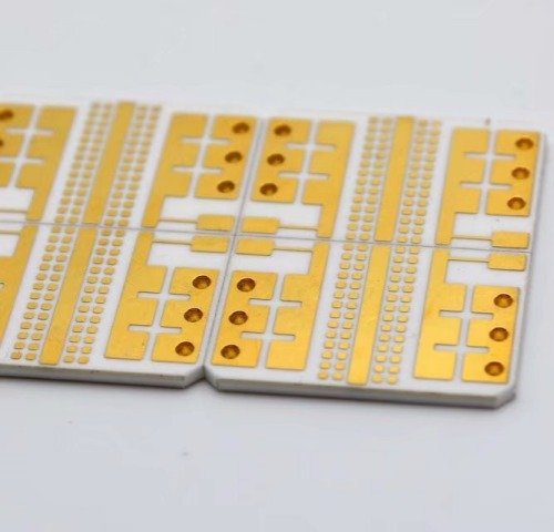
A custom carrier may use bonded or brazed copper, plated metallization or another construction suitable for its features and assembly. The choice affects available conductor geometry, thickness, finish and the way the device attachment is performed. Review the actual DBC process and AMB process options instead of combining their most favorable catalog properties into a nonexistent stack. Specify which surface supports die attachment and which supports interconnection. Ask how the supplier verifies the critical interfaces and dimensions for the proposed construction. A material substitution that preserves nominal conductivity may still change attachment compatibility or mechanical behavior, so it needs a broader review than replacing one number in a thermal calculation.
Examine mounting tolerance before reducing interface thickness
A thinner thermal interface can reduce an ideal conduction contribution, but the assembly must still accommodate actual surface geometry and meet its electrical requirements. Identify the tolerances that determine the gap at each device or substrate position, including part flatness, mounting features and cooler geometry. Do not reduce a nominal thickness without checking the minimum and maximum resulting conditions. A package-specific mounting solution should not be transferred to a bare ceramic carrier without validation. Define the mounting procedure and evidence supporting its loads through the responsible mechanical design process. The useful objective is a repeatable interface that satisfies the complete assembly requirements, not the smallest gap that can be produced on one carefully adjusted laboratory specimen.
Separate environmental cycling from active power cycling
An environmental temperature cycle and an electrically driven power cycle can create different temperature distributions and stresses in the assembly. Select qualification conditions from the product's expected exposures and failure mechanisms rather than treating all cycling as one interchangeable test. Record the temperatures or power conditions, dwell or timing, mounting arrangement and failure criteria. A reported cycle count without those details cannot establish equivalence between substrates. Use the thermal-cycling guide to organize the record and connect observations to the interfaces under investigation. A material's favorable toughness or conductivity can support a design choice, but neither property by itself demonstrates the completed charger's required service life.
Plan prototype evidence around the remaining uncertainty
If the main uncertainty is local heat spreading, measure or model the relevant spatial temperature behavior rather than testing only overall efficiency. If it is mounting repeatability, compare controlled assembly repetitions and their resulting thermal behavior. If it is the metallization interface, choose inspection and exposure that address that interface. Preserve specimen identity, material and process revisions, and the actual test fixture with the results. Avoid selecting only the best unit as representative of the design. A prototype program is more useful when each test can confirm or challenge a stated assumption. It should reduce a specific uncertainty before the carrier is released, rather than accumulating unrelated measurements that happen to be available.
Compare system cost rather than ceramic price alone
The substrate price is one contribution to the power-stage cost. Include device attachment, interconnection, cooler integration, inspection, yield assumptions and the work needed to qualify a new construction. A more expensive carrier could simplify a particular assembly, while a low-cost carrier could remain the better choice when it already meets the thermal and reliability requirements. Neither outcome should be assumed. Compare alternatives using the same delivered function and evidence requirements. Keep development charges and recurring costs separate, and distinguish an established production route from an experimental option. The ceramic PCB cost guide helps identify these categories without inventing a universal price premium for a named material.
Release a carrier specification that preserves the design logic
The release package should identify the supported stage, loss cases, ceramic and conductor construction, attachment surfaces, cooling boundary, electrical isolation responsibilities and acceptance evidence. Retain the calculation showing why the selected construction meets the design target, including uncertainties that remain. State which changes require renewed verification, such as a semiconductor substitution, different copper pattern, new interface material or revised cooler. Do not claim a component qualification automatically transfers to a custom carrier or to the completed charger. A controlled specification allows manufacturing and later design teams to understand the reason for the ceramic choice and reproduce the required assembly behavior rather than preserving a material name while inadvertently changing the conditions that made it work.
Engineering example
All efficiency, loss allocations, temperature targets and resistances are invented for screening arithmetic. They do not specify a semiconductor rating, insulation design or qualified onboard-charger operating condition.
Before you release the design
- Map losses to their physical stage and device positions.
- Distinguish module substrate from separate ceramic isolation plate.
- Keep thermal reference points and electrical potentials explicit.
- Review mounting, conductor layout and attachment together.
- Qualify the actual assembly and document change triggers.
Sources and further technical reading
Manufacturer references support the material and process context. Worked examples and checklists are engineering guidance; they are not test results or supplier guarantees.