
| Hypothetical input or result | Value | Meaning |
|---|---|---|
| LED count × voltage × current | 12 × 3.0 V × 0.70 A | 25.2 W electrical input |
| Assumed optical fraction | 35% | 8.82 W leaves as optical power |
| LED heat | 16.38 W | Electrical input minus optical output |
| Other on-board loss | 0.80 W | Illustrative additional heat |
| Shared path estimate | 17.18 W × 2.0 K/W | 34.36 K at defined path boundary |
Specify the array as an assembly
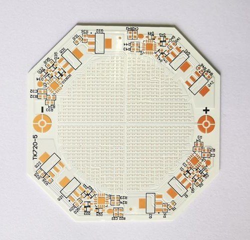
A useful ceramic LED array drawing describes more than the substrate material and board outline. It identifies the emitters, their electrical grouping, optical positions, attachment surfaces, thermal boundary and mounting arrangement. Those details determine whether a fabricator can make the board and whether an assembler can deliver the intended light source. Use the ceramic LED board guide for the construction options, then build a controlled specification that connects each requirement to an observable feature or an agreed test. A material name alone cannot establish array performance.
Freeze the LED package and land-pattern revision
Record the complete LED part number and the manufacturer's applicable package drawing. Distinguish electrical contacts from a dedicated thermal pad, and confirm the electrical status of that pad from the component documentation. Do not infer isolation because a pad is described as thermal. Include orientation, polarity, reference designators and the approved land pattern in the fabrication and assembly data. If alternative emitters are allowed, review their footprints and pad functions individually. Similar optical dimensions or marketing names do not guarantee interchangeable mounting geometry. Keep the component revision linked to the board revision.
Budget heat instead of equating all electrical power with heat
For an LED, electrical input is forward voltage times current; emitted optical power leaves the device as light rather than becoming heat at the junction. The heat estimate therefore depends on the optical conversion at the operating point. Cree LED's thermal guidance explicitly separates these quantities and uses stated assumptions for screening. For a real design, obtain suitable component data or measurements and retain the assumptions in the calculation. If usable optical power data are unavailable, treating all input as heat can be a conservative preliminary bound, but label it accordingly and include other losses that occur on the board.
Worked array heat-load example
Consider twelve hypothetical LEDs operating at 3.0 V and 0.70 A each. Electrical input is 12 × 3.0 × 0.70 = 25.2 W. Assume for this example that 35% leaves the LEDs as optical power, giving an estimated LED heat load of 16.38 W. If an additional 0.80 W of circuit loss is dissipated on the same board, the board-level heat load is 17.18 W. An assumed 2.0 K/W board-to-ambient path would then produce a 34.36 K rise at that path's reference point. This is not junction temperature: each emitter still has package and local spreading contributions, and the shared path may not be represented accurately by one resistance.
Define the cold-side interface and the measurement boundary
State whether the board is soldered, bonded, clamped through an interface material or integrated with another carrier. Identify the controlled surface, available contact area, mounting locations and the thermal test boundary. A ceramic layer calculation only covers one contribution. The thermal-resistance tool can show the effect of thickness, area and conductivity, while the thermal-management guide explains the complete path. Ask how the supplier will measure a result called board thermal resistance; without named temperature points and heat input, two quoted values may describe different quantities.
Keep current control separate from the substrate decision
Draw the actual series strings and any parallel branches, including connectors and return paths. Specify the intended driver current and the operating-voltage range using the approved LEDs. Parallel branches require an intentional current-sharing approach; ceramic conductivity does not control how current divides. Include failure behavior in the system review, such as the effect of an open emitter or a bypass device. Identify which resistors, protective parts or drivers dissipate heat on the array itself. This topology record also makes production testing clearer because continuity and polarity can be checked against defined circuit nodes.
Dimension optical locations from usable datums
If a lens, reflector or optical fixture references the board, define the same datum system across the mechanical and assembly drawings. A positional requirement can depend on board outline tolerance, fiducial registration, placement accuracy and the LED package's own optical-center relationship. List those contributions rather than assigning the whole error allowance to the bare ceramic. For a simple illustrative worst-case chain of ±0.05 mm board registration, ±0.04 mm placement and ±0.03 mm package offset along one axis, the sum is ±0.12 mm. A statistical combination requires evidence about distributions and independence; do not use it merely to obtain a smaller number.
Specify attachment quality with the operating consequence in mind
State the approved finish and attachment process, the regions requiring inspection, and how a defect affects acceptance. A single total-void percentage may not describe the location of a thermal obstruction beneath a concentrated source. Avoid inventing a universal criterion for every LED package or joining method. Obtain the component and assembly process recommendations, agree the inspection method, and connect the limit to thermal and reliability evidence. Cree LED's PCB thermal study demonstrates why local heat spreading and actual assembly measurements matter; its FR-4 and metal-core examples are not ceramic manufacturing limits to copy directly.
Build an acceptance test that can be repeated
Define drive current, ambient conditions, fixture or heat-sink configuration, stabilization criterion and temperature measurement location. Include optical measurements only with stated geometry and instrumentation. Test the expected hottest region, not only the most accessible pad, and document the method used to estimate junction temperature if that is an acceptance item. Preserve the LED lot and board revision with the results. The LED application guide provides system context; the final purchase specification should identify which tests the supplier performs and which belong to the completed luminaire or optical system.
Send one consistent release package
Bring the outline, conductor data, LED bill of materials, circuit topology, assembly drawing and acceptance requirements into the same revision-controlled package. Identify which dimensions are critical and which material or process substitutions need approval. Include required quantities and the state of delivery: bare board, populated array or mounted assembly. Use the RFQ brief builder to organize the handoff, but attach the controlled drawings that establish the design. Resolve contradictions before quoting so that a lower price does not simply reflect a different interpretation of the product.
Separate the bare-board purchase from the assembled-array purchase
Write down the physical state of the delivered product before comparing quotations. A bare metallized ceramic, an array with attached LEDs and an array already mounted to a cooler are different deliverables. The party supplying the bare board cannot demonstrate final optical alignment without the emitter and assembly process. Likewise, a populated array tested on an excellent laboratory heat sink does not establish performance in the customer's enclosure. Assign each acceptance item to the party able to perform it and identify the fixture needed. Include whether the price covers emitter procurement, attachment material, inspection, electrical test and packaging. This division avoids a common specification gap in which each supplier assumes another party will verify the completed thermal path.
Define the electrical measurement at the array terminals
Specify which terminals define the array input and whether driver losses are inside or outside that boundary. In a series string, the voltage at a connector includes conductor and contact drops as well as emitter voltages. If heat is estimated from measurements, record current and voltage at consistent points and identify any dissipating component excluded from the board. A supply display is not automatically a measurement at the array. For pulsed operation, distinguish instantaneous on-state power, average power and the duty cycle used to compute it. Current overshoot and pulse shape may matter to component limits even when average input looks acceptable. Retain the measured waveform or the controlled driver settings when a pulsed test is part of acceptance.
Examine unequal heating before averaging the array
The twelve-emitter example uses equal electrical conditions and an assumed optical fraction for every emitter. A real array may have unequal forward voltage, optical efficiency or local cooling. The hottest device therefore need not be the one nearest the geometric center, and average board temperature does not identify the maximum junction temperature. For an initial model, assign a heat source to each emitter and retain the location of nearby resistors or protection devices. Compare at least the normal operating pattern and a plausible uneven loading condition identified by the circuit design. If only part of the array is energized during some operating modes, analyze that spatial pattern as well. A lower total power does not automatically mean every local temperature is lower under a changed cooling or drive condition.
Use optical requirements that the proposed test can establish
Specify whether the product requirement is total radiant output, luminous output, illuminance at a plane or a spatial distribution. These are different quantities and cannot be substituted without the spectral and geometric information needed for the conversion. State the detector arrangement, working distance and stabilization conditions where relevant. If a secondary optic determines the final beam, decide whether array acceptance measures the bare emitters or the completed optical assembly. Record allowed emitter bins or other procurement constraints using the actual component definitions. Do not promise a final luminaire output solely from a sum of nominal component values. The purpose of the array test is to establish a defined and repeatable quantity that can be related to the system requirement.
Make a tolerance budget that follows the optical datum chain
Begin at the feature used to locate the optical assembly and follow the chain to the actual light-emitting region. Board outline, mounting-hole location, fiducial registration, placement and component construction can each contribute. Determine whether a common offset moves all emitters together or whether independent placement variation changes emitter-to-emitter spacing. Those two errors can have different optical consequences. A fixture that references mounting holes may be insensitive to an outline error but sensitive to hole-to-fiducial registration. Avoid adding every drawing tolerance indiscriminately when it is outside the functional chain. Conversely, do not omit a contribution merely because it belongs to a purchased component. Have the optical and assembly drawings reference compatible datums so that the budget describes the manufactured product.
Choose a thermal test point without hiding its limitation
A temperature measured on accessible copper is useful only when its relationship to the required device temperature is understood. A thermocouple can alter a small local thermal path, while an infrared reading depends on the measured surface and its optical behavior. Define preparation and attachment methods consistently and document where the sensor is located relative to the emitter. If a manufacturer provides a junction-temperature estimation method for the selected package, use its specified conditions and uncertainty rather than treating an arbitrary board reading as junction temperature. Compare repeated assemblies and repeated sensor installations when the acceptance margin is small. A stable reading at a convenient location is not evidence that the least accessible emitter is within its limit.
Design the mounting review around the real mechanical load path
Show how the ceramic assembly is supported while the cold-side interface is established. Identify the fastening or bonding locations and the areas that must remain clear for tools, optics and wiring. A metal fixture may distribute load differently from a final plastic housing, even if both use the same nominal screw locations. Ask the mechanical owner to define the approved mounting procedure and the evidence behind it. Do not assign a generic fastener torque to a brittle substrate without the relevant assembly specification. Also consider whether connectors or cables transmit force to the board after installation. Strain relief and access for assembly can be part of the array design rather than problems discovered after the optical layout is frozen.
Make changes and field replacements traceable
An approved alternative LED can change electrical voltage, optical distribution, attachment geometry or thermal behavior even when it fits the existing pads. Define which substitutions require design approval and which checks must be repeated. Preserve the array drawing revision, emitter lot identification where available and the test configuration with the acceptance record. If a replacement array must match an installed optical system, state the compatibility requirement instead of assuming that all nominally similar emitters are interchangeable. The same discipline applies to changes in finish, attachment material or cooling interface. A compact change matrix linking each changed feature to its required verification is more useful than a broad statement that the replacement is equivalent in every respect.
Engineering example
All values are hypothetical. The heat balance yields 17.18 W on the board. A shared-path temperature rise cannot by itself establish any individual LED junction temperature, optical output or lifetime.
Before you release the design
- Freeze LED part numbers, package drawings and pad electrical functions.
- Record string topology, drive conditions and on-board losses.
- Separate optical output from heat in the thermal budget.
- Align optical, mechanical and placement datum definitions.
- Agree repeatable assembly, thermal and optical acceptance methods.
Sources and further technical reading
Manufacturer references support the material and process context. Worked examples and checklists are engineering guidance; they are not test results or supplier guarantees.